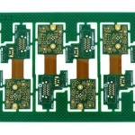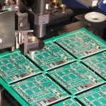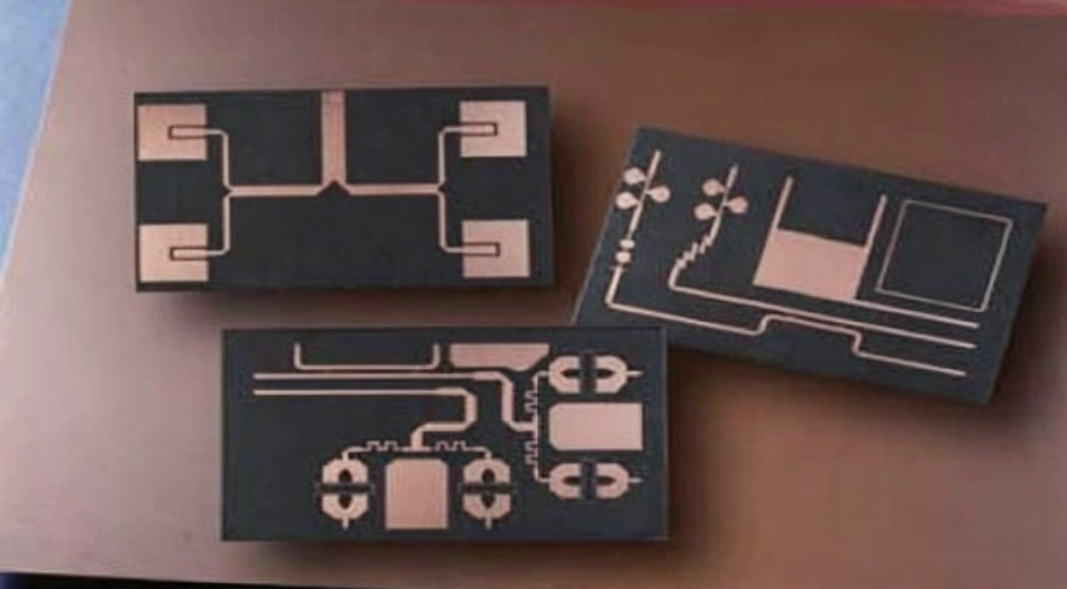
As the processing speed of microprocessors, signal converters, and high-speed data transmission equipment continues to increase, digital systems are reaching data rates of 100 Gbps and beyond. At these speeds, conventional PCB materials may no longer provide the electrical performance required for reliable high-speed signal transmission.
Therefore, selecting the appropriate High-Speed PCB Materials has become a critical part of high-speed PCB development. Material selection directly affects signal integrity, impedance control, insertion loss, thermal performance, manufacturing reliability, and overall product cost.
For high-speed and high-frequency designs, especially applications operating in the GHz range, PCB designers cannot select materials based solely on availability or price. The electrical, thermal, mechanical, and manufacturing characteristics of the material must all be evaluated.
Why PCB Material Selection Matters for High-Speed Circuits
In low-speed digital circuits, the influence of PCB material properties may be relatively limited. However, as signal rise times become shorter and operating frequencies increase, the PCB itself becomes an important part of the electrical transmission path.
A signal traveling through a PCB trace interacts continuously with the dielectric material and copper conductor. Material properties such as dielectric constant, dissipation factor, copper roughness, and dimensional stability can therefore have a direct impact on signal behavior.
For example, conventional FR-4 materials can exhibit relatively high dielectric loss at several GHz, depending on the specific resin system and material grade. Although FR-4 remains suitable for a wide range of electronic products, it may not be the optimal choice for demanding high-speed or high-frequency applications.
This is why selecting the right High-Frequency PCB Materials should be considered during the early stages of product development rather than after the PCB layout has already been completed.
Key Factors in PCB Material Selection
The selection of High-Speed PCB Materials should balance three major considerations:
- Electrical performance
- Manufacturing and reliability requirements
- Cost and production volume
A material with excellent electrical performance may not necessarily be the most suitable choice if it is difficult to manufacture, has poor thermal reliability, or significantly increases production costs.
The objective is to select a material that provides sufficient performance while maintaining stable manufacturing and acceptable overall cost.
1. Manufacturability and Reliability
Manufacturability is one of the most important factors when selecting a PCB Material Selection strategy.
A material may have excellent electrical specifications but still create manufacturing problems if its lamination characteristics, dimensional stability, or mechanical properties are unsuitable for the PCB structure.
Important manufacturing and reliability parameters include:
- Lamination behavior
- Resin flow characteristics
- Glass transition temperature (Tg)
- Decomposition temperature (Td)
- Thermal expansion characteristics
- Z-axis expansion
- CAF resistance
- Peel strength
- Mechanical strength
- Moisture resistance
- Flame-retardant performance
- Thermal cycling reliability
For multilayer PCBs, lamination behavior is particularly important. The resin system must provide sufficient bonding while maintaining the required dielectric thickness and structural stability.
For high-layer-count boards, material compatibility between different dielectric constructions should also be considered.
CAF Resistance
Conductive Anodic Filament (CAF) resistance is particularly important in high-density PCB applications.
As trace spacing and via spacing become smaller, the risk of electrical migration between conductive structures increases. A material with good CAF resistance can help improve insulation reliability under elevated temperature and humidity conditions.
Therefore, CAF performance should be evaluated when designing high-density and high-reliability products.
2. Electrical Performance
Electrical performance is the most important consideration for many High-Speed PCB applications.
Several material parameters have a direct impact on signal integrity.
Dielectric Constant (Dk)
The dielectric constant, or Dk, affects signal propagation velocity and transmission-line impedance.
For a simplified transmission-line structure, changes in dielectric constant can alter the effective electrical length and impedance.
This means that variations in Dk can cause impedance deviations between the designed PCB and the manufactured PCB.
For high-speed interfaces, stable Dk across frequency and temperature is therefore important.
Dissipation Factor (Df)
The dissipation factor, or Df, represents dielectric loss.
As frequency increases, dielectric loss becomes increasingly important because high-frequency signals experience greater attenuation while traveling through the PCB.
Lower Df materials generally provide lower dielectric loss and can be beneficial for long high-speed transmission paths.
However, Df should not be considered independently. The complete insertion loss of a PCB channel also depends on conductor loss, copper roughness, geometry, frequency, and other factors.
Dk and Df Stability
For demanding high-speed applications, the nominal Dk and Df values are not enough.
Designers should also consider:
- Frequency-dependent Dk
- Dk tolerance
- Df stability
- Temperature dependence
- Moisture dependence
- Resin content variation
- Dielectric thickness tolerance
A material with stable electrical characteristics can make impedance design and simulation more predictable.
3. Impedance Control
Impedance Control is essential for high-speed digital and RF transmission lines.
Interfaces such as PCIe, Ethernet, USB, SerDes, and other high-speed links may require carefully controlled single-ended or differential impedance.
PCB impedance depends on multiple factors, including:
- Trace width
- Trace thickness
- Dielectric thickness
- Dielectric constant
- Copper roughness
- Trace geometry
- Reference-plane configuration
Therefore, material selection and PCB stack-up design should be considered together.
For example, if the dielectric thickness varies significantly during manufacturing, the resulting impedance may deviate from the design target even when the trace width is manufactured correctly.
This is why material thickness and resin content tolerances are important for high-speed PCB manufacturing.
4. Copper Roughness
Copper roughness becomes increasingly important as signal frequency increases.
At high frequencies, current tends to concentrate near the surface of the conductor due to the skin effect. As a result, the actual copper surface profile can influence conductor loss.
For long high-speed transmission lines, designers should consider copper foil roughness as part of the overall loss budget.
Smoother copper can help reduce certain high-frequency conductor losses and improve signal transmission performance. However, copper roughness must also be evaluated together with adhesion, peel strength, manufacturability, and reliability.
Therefore, the goal is not simply to choose the smoothest copper available, but to select a copper surface that provides an appropriate balance between electrical performance and manufacturing reliability.
5. Thermal Performance
High-speed processors and communication devices often generate substantial heat.
As system power density increases, PCB material selection must also account for thermal reliability.
Important thermal parameters include:
- Tg
- Td
- Z-axis expansion
- Thermal conductivity
- Coefficient of thermal expansion (CTE)
- Thermal cycling performance
A PCB material with insufficient thermal stability may experience dimensional changes, delamination, cracking, or other reliability problems during repeated thermal cycles.
For high-layer-count boards and high-power applications, the thermal properties of the material should therefore be evaluated during stack-up design.
6. Dielectric Thickness and Resin Content
The dielectric thickness between a signal layer and its reference plane directly affects transmission-line impedance.
In multilayer PCB manufacturing, the final dielectric thickness is influenced by core thickness, prepreg selection, copper thickness, resin content, lamination pressure, and lamination temperature.
For this reason, the nominal material thickness specified in a datasheet does not always represent the final dielectric thickness after fabrication.
Designers should work with the PCB manufacturer to establish an appropriate stack-up and verify the final construction.
For High-Speed PCB Materials, tight thickness control can be particularly important for differential pairs and other impedance-controlled structures.
7. Frequency and Environmental Stability
High-speed signals do not operate at only one idealized frequency.
Real digital signals contain a wide range of frequency components determined largely by their rise and fall times. Therefore, material behavior across a broad frequency range should be considered.
Environmental conditions can also affect electrical performance.
Changes in:
- Temperature
- Humidity
- Material moisture absorption
- Mechanical stress
- Frequency
may cause changes in dielectric properties and transmission-line behavior.
For high-reliability products, designers should therefore evaluate material stability under the expected operating environment rather than relying only on room-temperature datasheet values.
8. Simulation Before PCB Layout
Simulation should be performed during the early stages of High-Speed PCB development.
Before finalizing the PCB stack-up and routing, designers can use signal-integrity simulation to evaluate:
- Impedance
- Insertion loss
- Return loss
- Crosstalk
- Reflection
- Eye diagrams
- Differential-pair behavior
- Channel operating margin
Simulation results provide an important reference for selecting materials and establishing the PCB stack-up.
For example, if a long high-speed channel produces excessive insertion loss, the designer may need to evaluate lower-loss High-Frequency PCB Materials, smoother copper, shorter routing paths, improved connector transitions, or other channel-level improvements.
Material selection should therefore be driven by actual system requirements rather than by datasheet specifications alone.
9. Cost and Production Volume
Cost is another important consideration when selecting High-Speed PCB Materials.
Advanced low-loss laminates can provide better electrical performance but may cost significantly more than standard FR-4 materials.
The appropriate material depends on the product’s actual requirements.
For example:
- Low-speed control boards may use standard FR-4.
- Moderate-speed digital products may require improved FR-4 or mid-loss materials.
- High-speed networking equipment may require low-loss or very-low-loss materials.
- RF and microwave products may require specialized high-frequency laminates.
Production volume also affects the overall cost balance. For high-volume products, material availability, supply stability, manufacturing yield, and process compatibility may be as important as the material’s nominal electrical performance.
How to Choose the Right High-Speed PCB Material
A practical material-selection process can follow these steps:
Step 1: Define the Signal Requirements
Determine the data rate, interface type, signal rise time, operating frequency range, channel length, and allowable insertion loss.
Step 2: Establish the Electrical Targets
Define the required Dk, Df, impedance, loss budget, and differential-pair requirements.
Step 3: Evaluate Thermal and Reliability Requirements
Consider operating temperature, thermal cycling, Tg, CTE, CAF resistance, moisture resistance, and expected product lifetime.
Step 4: Develop the PCB Stack-Up
Select core and prepreg constructions that provide the required dielectric thickness and impedance characteristics.
Step 5: Simulate the High-Speed Channel
Perform signal-integrity and, when necessary, power-integrity simulations before finalizing the design.
Step 6: Confirm Manufacturing Capability
Work with the PCB manufacturer to verify whether the selected material, stack-up, trace geometry, drilling, plating, and impedance tolerances can be manufactured consistently.
Step 7: Balance Performance and Cost
Choose the material that meets the actual system requirements without unnecessarily increasing manufacturing costs.
Kingda’s Approach to High-Speed PCB Manufacturing
The performance of High-Speed PCB Materials depends not only on the material itself but also on how the PCB is designed and manufactured.
Kingda can support high-speed PCB projects by coordinating material selection with stack-up design, controlled impedance, precision fabrication, and manufacturing process control.
Key considerations include:
- High-speed and high-frequency PCB fabrication
- Controlled impedance manufacturing
- Multilayer stack-up optimization
- Low-loss material processing
- Fine-line PCB manufacturing
- Precision drilling and plating
- Copper surface control
- Signal-integrity considerations
- Electrical testing and quality inspection
Early communication between the PCB designer and manufacturer can significantly reduce manufacturing risks and improve first-pass success.
Conclusion
Choosing the right High-Speed PCB Materials is essential for reliable high-speed digital and high-frequency applications.
The selection process should consider much more than dielectric constant and dielectric loss. Dielectric Constant (Dk), Dissipation Factor (Df), Impedance Control, Copper Roughness, dielectric thickness, thermal performance, CAF resistance, dimensional stability, manufacturability, and cost all need to be evaluated together.
For 100 Gbps and other demanding high-speed applications, PCB material selection should begin during the early design stage. Combining material evaluation, stack-up optimization, signal-integrity simulation, and close cooperation with the PCB manufacturer allows engineers to achieve a better balance between electrical performance, reliability, manufacturability, and cost.
With the right material and a properly controlled manufacturing process, Kingda can help customers develop high-speed PCB solutions that meet demanding signal-integrity and reliability requirements.