AI Backplane PCB: High Layer Count Manufacturing Guide
Why AI Racks Depend on the Backplane PCB
AI model training, high performance computing and cloud data centers are turning server racks into dense computing systems. GPU training clusters, AI inference servers and hyperscale data centers all rely on high speed, high reliability backplane interconnect, and at the center of every AI rack sits the backplane PCB. The board carries high speed data between devices, distributes power and links every compute module, which is why engineers often call it the neural center of the AI server.
With PCIe 5.0, PCIe 6.0, CXL, 400G and 800G switching and GPU clusters becoming standard, ordinary boards can no longer support ultra high speed transmission. More AI systems are moving to 24 layer, 36 layer, 48 layer, 60 layer and even 78 layer orthogonal backplane PCBs to reach higher bandwidth with lower loss and stronger reliability. This guide explains how AI backplane PCBs are structured, which materials are used, how they are manufactured and tested, what they cost and what design steps improve yield.
gopcb manufactures high layer count AI backplane PCBs through its PCB manufacturing service.
What Is an AI Backplane PCB?
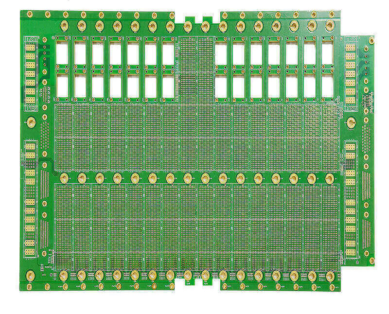
An AI backplane PCB is a large multilayer board that connects the functional modules inside an AI server rack. Typical connection targets are GPU accelerator cards, CPU compute boards, AI training modules, network switches, storage systems, power distribution units and optical module interfaces.
The backplane does not compute by itself. Its job is to exchange data and distribute power across the rack. In a large training cluster a single backplane may support thousands of high speed differential signal channels, and its performance directly decides the bandwidth and stability of the whole machine. Current mainstream protocols include PCIe Gen 5 and Gen 6, NVLink, CXL, InfiniBand, and 400G and 800G Ethernet, which places extreme demands on signal integrity.
Why AI Racks Need High Layer Count Boards
More GPUs per system. Traditional servers carry two to four CPUs, while AI training servers commonly hold 8, 16 or 32 GPUs or multi node clusters. Every GPU needs many high speed links, which multiplies the routing resources required on the board.
Faster data rates. AI servers now operate at 56G and 112G PAM4 and are moving toward 224G PAM4. The higher the rate, the stricter the design and fabrication tolerances, from dielectric loss to via stubs and surface roughness.
More complex power systems. Accelerator cards consume 700 W for an H100 and more than 1000 W for a B200 class GPU, so a single rack can draw 10 kW, 20 kW or even 50 kW. That requires many power and ground planes to keep the supply stable under load.
High density connectors. AI backplanes use high speed, orthogonal and mezzanine connectors, and every connector needs more routing and reference layers around it. This is why 24, 36, 48, 60 and 78 layer orthogonal backplanes have become mainstream.
Typical Stack-up of an AI Backplane PCB
A 48 layer high speed backplane typically includes 24 signal layers, 12 ground layers and 12 power layers. The design goals focus on three areas.
Impedance control. Common requirements are 50 ohm single ended, 85 ohm differential and 100 ohm differential with tolerances usually held within plus or minus 5 percent, which demands uniform line widths, dielectric spacing and stack-up control.
Crosstalk reduction. Ground reference layers and isolation planes reduce near end and far end crosstalk so every high speed pair keeps clean margins.
Power integrity. Multiple power planes lower voltage droop and noise, improving GPU supply stability during compute bursts.
Materials for AI Backplane PCBs
Material selection determines high speed performance. Standard FR-4 suits mid and low speed servers and industrial controls thanks to low cost and mature processing, but its higher loss does not support 800G class links. Mid loss materials such as Panasonic Megtron 6, Isola I-Speed and EM-888 give lower dielectric loss, better signal integrity and higher reliability for 400G network equipment and AI inference servers. Ultra low loss grades serve 800G switches, AI training clusters and HPC supercomputers.
Common advanced families include Megtron 6, Megtron 7, Tachyon 100G and Rogers high speed laminates. For backplane applications the copper foil roughness matters as much as the resin system, because rough foil increases conductor loss at high frequency. Specifying the material family early avoids expensive stack-up changes later.
Manufacturing Process for High Layer Count Backplanes
Producing a 48 layer or higher backplane is one of the most demanding jobs in PCB fabrication. Inner layers are imaged with tight registration, laminated under controlled pressure and temperature, and drilled with precision equipment that handles thousands of holes across a large panel.
Back drilling removes the unused via stubs that would otherwise reflect high speed signals, which is essential for 112G and 224G performance. Plating, imaging and etching continue layer by layer, and the surface finish is normally ENIG or hard gold. ENIG protects the pads and provides a flat solderable surface, while hard gold is applied in connector and gold finger areas for wear resistance in frequently mated AI rack systems.
Every board then passes electrical and reliability testing before shipment. AOI checks open and short circuits, notches and residual copper. Flying probe verifies connectivity and electrical performance on prototypes. X-ray inspects buried via quality and multilayer registration, TDR validates impedance and signal continuity, and thermal cycling, IST, solderability and thermal shock tests confirm long term operation.
Manufacturing Challenges
High layer backplanes push every process to its limit. Registration error on boards above 48 layers must stay below about 75 micrometers, which demands precision tooling and careful lamination control. Warpage is tightly limited to about 0.5 percent or less on boards that reach 600 mm, 800 mm or more than 1000 mm, so asymmetric copper distribution must be avoided in design. Signal loss depends on copper foil roughness, dielectric loss and via structure, and can only be solved by combining material and process optimization.
Yield management is the biggest business risk. Higher layer counts mean more process steps and more chances for defects, so manufacturers rely on AOI, statistical process control, DFM review and full traceability to keep yield stable. Choosing a partner with real experience in large backplanes is therefore more important than comparing unit prices.
AI Backplane PCB Cost Reference
Pricing depends on layer count, board size, material brand, back drill structure and quantity. Prototype samples of 1 to 5 pieces run roughly 1500 to 5000 USD for 24 to 36 layer boards, 4000 to 12000 USD for 48 to 60 layer boards, and 10000 to 30000 USD or more for 78 layer orthogonal designs. Small batch production of 10 to 100 pieces falls to about 800 to 8000 USD per board, while volume orders are quoted by annual quantity, material plan and process complexity.
Because these boards are expensive, an early PCB design and layout review prevents costly changes. Design engineers should prefer back drill structures, reduce via transitions, optimize differential routing, fix the material plan early and add test coupons so impedance can be verified in production.
FAQ
How many layers does an AI backplane PCB use? Mainstream AI backplanes run from 24 to 60 layers, and high end systems use 78 layer orthogonal designs.
Why does high speed PCB need back drilling? Back drilling removes via stubs that cause signal reflection, improving signal quality for 112G and 224G links.
Which materials do AI servers use? Megtron 6, Megtron 7, Tachyon 100G and Rogers high speed materials are the mainstream choices for high layer AI boards.
What surface finish is used on AI backplanes? ENIG and hard gold are the most common. ENIG protects pads and hard gold adds wear resistance in connector and gold finger zones.
How long does high layer backplane production take? Prototypes normally need 15 to 25 days, small batches about 20 to 35 days, and volume lead times depend on project scale.
Get an AI Backplane PCB Quote
AI training, GPU clusters, 800G switching and next generation data centers are making high layer backplane PCBs one of the most important technologies in computing infrastructure. Every link in the chain, from material and stack-up to impedance control, back drilling and reliability testing, directly affects server performance and stability. gopcb provides orthogonal backplane manufacturing, ultra low loss material processing, back drilling, large board production, precise impedance control and IPC Class 2 and Class 3 quality. Send your stack-up and Gerber files for a DFM review and a custom AI backplane PCB quotation, backed by PCBA testing support for the complete rack system.