Embedded Copper Coin PCB: Design, Process and Thermal Performance
Why High Power Boards Need Embedded Copper Coins
Electric vehicles, AI servers, industrial power supplies, 5G base stations and high performance computing equipment are pushing more power through smaller boards every year. As MOSFET, IGBT, SiC and GaN devices increase in power density, thermal management has become the factor that decides whether a product lives or fails. Traditional solutions such as thermal vias, heavy copper and metal core laminates transfer heat layer by layer, and at today’s power levels that indirect path is no longer enough.
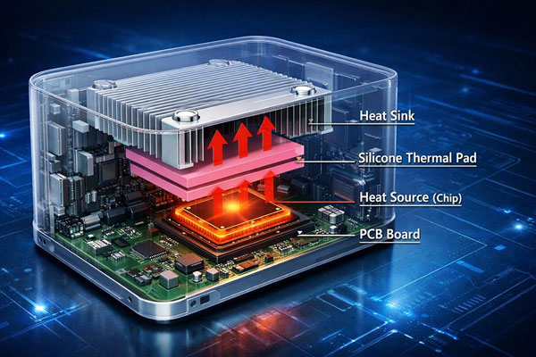
Embedded copper coin PCB technology solves the problem by placing a machined copper block directly inside the board structure under the hottest component. The coin creates a low resistance, high efficiency thermal channel that moves heat straight to a heatsink or metal housing, lowering junction temperature and improving stability and service life. This guide explains how embedded copper coins are designed, processed, priced and applied, and what to check before you send files to a manufacturer.
gopcb supports embedded copper coin PCBs from DFM review to volume production through its PCB manufacturing service.
What Is an Embedded Copper Coin PCB?
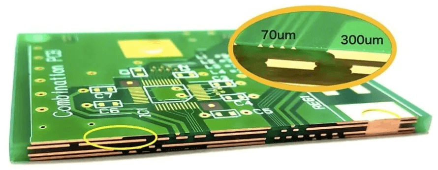
An embedded copper coin PCB is a printed circuit board with a precision copper block embedded inside its laminated structure. The coin sits directly under power components such as MOSFETs, IGBTs, CPUs and GPUs and carries heat from the device to a heatsink or enclosure without traveling through multiple dielectric layers.
Common coin thicknesses range from 0.5 mm to 3.0 mm, and custom designs can exceed 8 mm. Typical copper materials are C1100 high purity copper, OFHC oxygen free copper and high thermal conductivity copper grades with values around 390 to 400 W/m·K, roughly one thousand times the thermal conductivity of FR-4.
Why Use Copper Coin Technology?
Extremely high thermal conductivity. Copper conducts heat far better than ordinary PCB laminates. FR-4 measures about 0.3 W/m·K, aluminum base boards about 170 W/m·K, aluminum nitride ceramics 170 to 200 W/m·K, and copper 390 to 400 W/m·K, which is why the coin approach outperforms every dielectric-based solution for spot heat removal.
Higher power density. Embedded coins support larger operating currents, higher power output, smaller board size and denser component placement, which is exactly what EV powertrains and AI servers demand.
Much lower thermal resistance. Compared with thermal via arrays, the heat path is shorter, resistance is lower, cooling efficiency is higher and the heatsink is used more effectively because heat arrives at one flat, well defined surface.
Better mechanical strength. The copper block also stiffens the local board area, reduces warpage at high temperature and improves long term reliability under thermal cycling.
How Embedded Copper Coin PCBs Are Made
Copper coin boards belong to the advanced PCB process family and demand precise equipment and tight process control.
Step one: structure design. The engineer defines coin size and position, stack-up, copper weight, heat flow path, safety spacing and DFM rules so that the coin area is manufacturable and the thermal path is optimized before tooling starts.
Step two: CNC coin machining. High precision CNC machines produce the copper blocks with dimensional control around ±0.02 mm, holding flatness, surface roughness and consistency across the batch.
Step three: pocket milling. The core layer receives a pocket that matches the coin with tight size control, burr-free walls and enough resin fill space so lamination can capture the block without voids.
Step four: placement and lamination. The coin is inserted into the pocket and the stack is bonded under vacuum lamination. Vacuum pressure removes air and guarantees resin fills every gap around the coin, which is essential for both mechanical strength and thermal contact.
Step five: finishing and inspection. The board is drilled, plated, imaged and finished as usual, then inspected with X-ray, AOI and thermal or electrical testing to verify coin position, resin fill and final performance. Because a misplaced or voided coin cannot be repaired, inspection is treated as a critical quality gate.
Design Rules for Copper Coin PCBs
Copper coin PCB design follows a few rules that differ from ordinary multilayer layout. The coin must sit directly under the component pad or thermal land so the thermal path is short. The pocket wall clearance should be uniform to guarantee resin flow. Copper weight and coin thickness must be coordinated with the stack-up, and plating over the coin face must be planned if the surface is soldered or needs a specified finish.
Thermal vias can still be added around the coin to spread heat into adjacent copper planes, and ground planes around the cavity improve both shielding and heat spreading. Engineers should also allow a keep-out area for routing so that no signal trace is cut by the cavity, and should request a DFM check early because pocket position errors and thin dielectric walls are the most common causes of yield loss.

Materials and Combination Processes
Embedded copper coin technology works with a wide range of laminates. High Tg FR-4 covers most power boards. Ceramic filled or high thermal conductivity dielectrics improve heat spreading around the coin, and metal core boards can be combined with coins where the design needs both. The coin itself can be combined with HDI microvias, blind and buried vias, heavy copper and impedance control in one design, which is how modern high power boards achieve high density routing and strong cooling at the same time.
For very high power modules, copper coins are often paired with direct bonded copper (DBC) or insulated metal substrate sections, although for most OEM projects a well executed FR-4 board with coins delivers the best balance of cost, thermal performance and process maturity.
Applications of Embedded Copper Coin PCBs
The main users of copper coin boards are power dense systems where heat must leave through the enclosure. New energy vehicle inverters, on board chargers and BMS controllers use coins under their power switches. AI servers and data center power supplies embed coins under CPUs, GPUs, VRM stages and switch mode converters. Industrial automation and motor drives use them for servo amplifiers and high current drivers. Energy storage converters, communication base stations, medical electronics, high power LED lighting and aerospace power units all adopt the same technique when thermal via arrays are insufficient.
Embedded Copper Coin PCB Cost Reference
Pricing depends on layer count, coin size and number, material grade, process complexity and order quantity. Prototype boards typically range from 180 to 450 USD for two layers, 400 to 900 USD for four to eight layers, and 900 to 2000 USD or more for complex high layer designs with multiple coins. Small batch production of 50 to 500 pieces runs roughly 40 to 150 USD per board, while volume orders above one thousand pieces typically land between 8 and 60 USD per board.
The main price drivers are coin CNC machining, pocket milling, vacuum lamination, X-ray inspection, thermal resistance testing, material grade and the yield control needed to keep cavity defects low. A complete PCB design and layout review before tooling is the most effective way to keep those drivers under control. Requesting a quote with stack-up, coin drawing and thermal requirements gives the manufacturer everything needed for an accurate number. gopcb offers combined PCB assembly and fabrication so the coin board and its power stage can be built and tested under one roof.
FAQ
What is an embedded copper coin PCB? It is a PCB with a high thermal conductivity copper block embedded inside the laminate to move component heat directly to a heatsink or enclosure.
Is a copper coin better than thermal vias? For high power devices yes. The coin provides much lower thermal resistance and higher heat removal efficiency, making it the natural upgrade when via arrays saturate.
Which industries use copper coin PCBs? EV, AI servers, industrial automation, energy storage, communication base stations, medical electronics and high power LED applications are the main adopters.
How thick can an embedded coin be? Production normally supports 0.5 mm to 8 mm, with thicker custom blocks possible depending on stack-up and board thickness.
Can copper coin be combined with HDI? Yes. Advanced manufacturing combines coins with HDI, blind and buried vias, heavy copper and impedance control in a single design.
Get an Embedded Copper Coin PCB Quote
As high power electronics get smaller and denser, embedded copper coin technology has become one of the most effective thermal solutions in PCB manufacturing. It shortens the heat path, lowers junction temperature and improves system reliability for EV, AI, industrial, storage and communication products. gopcb manufactures 1 to 40 layer boards with copper weights from 0.5 to 20 oz, coin thicknesses from 0.5 to 8 mm, vacuum lamination, X-ray and functional test, and IPC Class 2 and Class 3 quality control. Send your files for a free DFM review and an embedded copper coin PCB cost estimate.