Half Hole PCB: Castellated Holes Design and Manufacturing Guide
Why Half Hole PCB Technology Is Growing
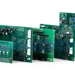
Electronics keep moving toward smaller size, modular architecture and higher integration, and PCB design must deliver both performance and easy connection. Half hole PCB technology, built on castellated holes, has become one of the key solutions for joining modules to main boards. A module with half holes can be soldered directly onto the host board like an SMT component, which is why it is used across IoT modules, wireless communication modules and embedded systems.
This guide explains what half holes are, how they work, how they are manufactured, which design rules keep them reliable, what they cost in 2026 and how to choose a supplier with real castellated hole process experience.
gopcb produces half hole boards through its PCB manufacturing service.
What Are Castellated Holes?
Castellated holes, also called half holes, are plated through holes that have been cut in half at the edge of the board. The structure has three defining features: it sits exactly on the board outline, the inner wall carries plated copper for conductivity, and the exposed shape is a semicircular opening that provides both electrical connection and mechanical fixing.
The difference from a normal via is fundamental. A regular via sits inside the board and carries signals between layers, while a half hole sits on the edge and connects the module to the outside world. That single difference makes castellations the natural interface for board to board assembly.
How Half Holes Work
Half hole PCBs create board to board connections in a way that is very close to SMT placement. The main board provides matching pads, the half hole module is aligned over them, solder paste is printed, and reflow soldering forms the joint. No connector is required, which saves space, cuts cost and improves reliability compared with traditional mezzanine or header connections.
Because the mechanical and electrical connection happens in the same solder joint, the quality of the plated half wall and the edge profile directly decide how strong and how conductive the module connection will be.
Half Hole PCB Manufacturing Process
Manufacturing a half hole board combines several high precision steps. Standard holes are first drilled at the board edge, then plated with copper in the PTH process so the hole wall becomes conductive. The circuit pattern is formed by imaging and etching, solder mask protects the non conductive areas, and profile routing then cuts the through holes in half along the board outline. A surface finish such as ENIG or HASL completes the board.
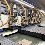
Profile routing is the core step and the main source of defects. The copper wall can be damaged during routing, the half hole edge must be smooth and burr free, and the plated copper thickness must stay uniform around the cut. A reliable factory uses precision CNC routing and stable plating control so every castellation comes out consistent.
Design Rules for Castellated Holes
Design is where half hole reliability is decided. Practical parameter guidance is a hole diameter of at least 0.6 mm, an annular pad ring of at least 0.25 mm, hole to hole spacing of at least 0.5 mm, and hole centers placed precisely on the board edge so the routed profile is symmetrical.
Best practice includes open window design so solder mask never covers the half hole area, evenly spaced castellations for good placement and soldering, fiducial markers for assembly alignment and optimized panelization to lower cost. Common mistakes are small holes that plate poorly, thin copper rings that weaken the solder joint and poor edge tolerance control that makes half holes asymmetric.

Design for testability also matters. Because castellations are the only electrical connection for many modules, a good layout adds test pads and clear fiducials so AOI and functional test can verify the module on the host board. Working through a complete PCB design and layout review at the start avoids edge tolerance and plating problems that are expensive to fix after tooling.
Advantages and Challenges
The advantages of half holes are clear. They save space for dense, small products, simplify assembly because no connector is needed, improve reliability through a solid mechanical and electrical connection and reduce system cost by removing connector and assembly steps in volume production.
The challenges are equally real. The process is more complex, precision demands are higher, routing can affect plated hole copper quality and unit cost is slightly above an ordinary PCB. These issues are manageable when the design follows the rules above and the manufacturer has mature castellated processing rather than treating the half hole as a special request.
Applications of Half Hole PCBs
Typical applications are IoT modules such as Wi-Fi and Bluetooth, RF communication modules, embedded systems, consumer electronics and industrial control equipment. Half hole design is especially suitable for products that need modular upgrades and fast integration, because a castellation module can be developed once and reused across many host designs.
Compared with edge plating, half holes are used for connection while edge plating is used for shielding or grounding. Compared with ordinary vias, half holes make external connections while vias route internally, and compared with SMT pads alone, half holes provide higher mechanical strength at the cost of slightly more complex design.
Half Hole PCB Cost Reference 2026
Price depends on layer count, material, hole size and tolerance, finish and quantity. A two layer prototype of 5 to 10 pieces typically runs 30 to 80 USD. Small batches of 50 to 100 pieces cost roughly 120 to 300 USD total, and large volume orders above 1000 pieces can fall to 0.05 to 0.30 USD per board as tooling is amortized. High frequency materials and multilayer stacks move pricing up in proportion to their normal premium.
For volume products the module cost saving from removing connectors usually outweighs the small per board premium, which is why half holes remain popular in IoT hardware. An accurate quote needs the Gerber, drill and outline files plus the required finish and tolerance. gopcb also supports the assembly side through its PCB assembly service so module and host board can be built and tested together.
How to Choose a Half Hole PCB Manufacturer
Evaluate whether the supplier has real half hole experience, CNC routing and plating capability, ISO and IPC based quality control, and responsive delivery. Castellations fail most often in plating and edge routing, so ask for process documentation and inspect the edge quality of a sample before committing to volume. A manufacturer with dedicated half hole production gives consistent hole copper, clean edges and competitive 2026 pricing.
FAQ
What is the minimum half hole diameter? Usually 0.6 mm, depending on the factory capability.
Are half hole PCBs reliable? Yes, with correct design rules and controlled manufacturing they provide very high connection reliability.
Can every factory make half holes? No. Castellated processing needs dedicated routing and plating capability.
Which files are needed for a quote? Gerber files, drill files and outline files, plus finish and tolerance requirements.
Why use half holes instead of a connector? Half holes save space, cut assembly steps and lower cost while giving a strong mechanical and electrical joint.
Get a Half Hole PCB Quote
Half hole PCB technology is a proven way to achieve modular design and high density integration, and it is widely used in IoT and wireless communication products. Higher manufacturing requirements are offset by design rules and a capable supplier, and smart hardware and IoT growth is making castellation a standard option for module design. gopcb specializes in high precision half hole PCB manufacturing with stable plating, controlled routing, ISO and IPC quality systems and competitive 2026 pricing. Send your Gerber and outline files for a free DFM review and a half hole PCB quotation today.