PCB Hole Copper: Plated Through Hole Process Guide
Why PCB Hole Copper Is a Core Manufacturing Skill
In modern electronics, PCB manufacturing is what keeps a circuit running reliably, and one of the most important yet often overlooked steps is hole copper plating. Whether the board is a multilayer design, a high speed signal board or an industrial control product, the copper inside every drilled hole affects electrical connection, mechanical strength and long term reliability. A board can have perfect traces on its surface and still fail early if its hole copper is thin, voided or cracked.
This guide explains what PCB hole copper is, why it matters, which types exist, how the plating process works, what thickness standards apply, which defects appear and what 2026 pricing looks like.
gopcb controls hole copper quality through its PCB manufacturing process with cross section and reliability verification.
What Is Hole Copper?
Hole copper is the layer of copper deposited on the inner wall of a drilled hole in the PCB. The plating process creates a conductive channel, usually called a plated through hole or PTH, so different circuit layers can be connected vertically. Hole copper exists only inside the hole wall while surface copper forms the traces on the outer layers, and the two are plated together in the same process sequence.
Good hole copper provides three things at once: vertical interconnection between layers, a stable current path and mechanical reinforcement of the hole wall so the barrel survives soldering and thermal cycling.
Why Hole Copper Matters
Electrical connection is impossible without it. In a multilayer board, signals cross layers through plated holes, so hole copper is the physical backbone of the interconnect.
Mechanical strength improves. High quality hole copper strengthens the bond between pads and hole walls, giving the board better resistance to thermal shock and vibration.
Signal integrity depends on uniformity. Even hole copper thickness helps maintain impedance stability and lowers signal loss, which is essential on high speed PCB designs where the via is part of the transmission channel.
Types of Plated Holes
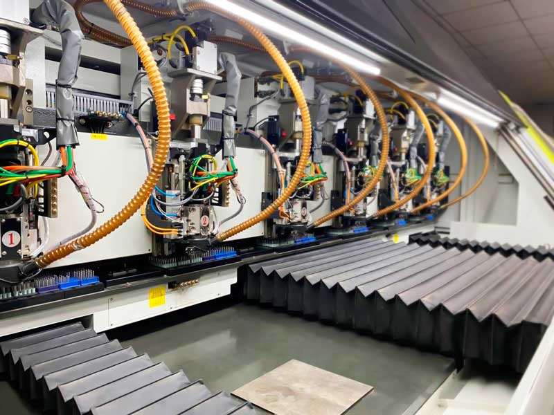
Through hole copper is the most common type and is used for component insertion and layer to layer connection. Via copper covers blind vias that connect outer layers to inner layers, buried vias that connect inner layers only, and microvias used on HDI boards. Plated holes can also be filled or unfilled. Filled vias improve reliability and are preferred for high end electronics, while unfilled vias cost less and suit conventional products.
The choice between these types sets the process difficulty. A blind or buried via needs sequential lamination, and a microvia demands laser drilling and tight plating control inside a very small barrel.
The PCB Hole Copper Plating Process
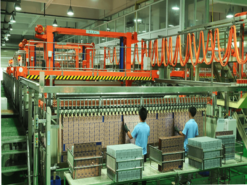
Plating follows a fixed sequence. Drilling first creates the hole with a mechanical or laser drill. Desmear then removes resin residue from the hole wall so the copper can adhere. Electroless copper deposits a thin conductive base layer, and electroplating thickens the copper to the required specification using controlled current. Inspection completes the cycle with cross section analysis and X-ray checks.
Every step affects the final quality. A poor desmear leaves resin on the wall, an unstable electroless bath creates skip plating, and uneven current density produces thin copper at the center of high aspect ratio holes.
Hole Copper Thickness Standards
The common reference standard is IPC-6012. Standard hole copper thickness is typically 20 to 25 micrometers, while high reliability applications specify 25 micrometers or more. Automotive, aerospace and medical programs hold stricter thickness and distribution limits because their boards face decades of thermal and mechanical stress.
Thickness is usually measured on a cross section at the thinnest point of the barrel, and both average and minimum values are reported. Specifying only a nominal number is not enough; the minimum wall thickness in the center of the hole is the value that determines reliability.
What Affects Hole Copper Quality
Aspect ratio is the main difficulty. The ratio of hole depth to diameter decides how hard it is to plate the center evenly, and high aspect ratio HDI holes are the hardest to keep uniform. Plating uniformity depends on the chemical bath, current density control and agitation, and any deviation creates thin zones inside the barrel.
Board thickness, hole size, copper weight and stack-up also interact with plating. A thick board with small holes needs longer plating time and better throwing power, which is why high layer count boards carry a visible cost premium.
Hole copper quality is also a design question. Choosing a sensible aspect ratio, specifying realistic hole sizes and avoiding unnecessarily deep small vias gives the plating process a wider window and higher yield. Reviewing the via strategy during PCB design and layout prevents the most common plating failures before the order reaches the factory.
Common Hole Copper Defects
Voids are the most dangerous defect because they reduce conductivity and can open the circuit later in life. Poor adhesion leads to delamination or failure at the hole wall, uneven thickness shortens reliability, and cracks appear under thermal cycling when the copper is too thin or the resin system moves too much. Each defect class needs a different root cause fix, from bath chemistry to drill parameters, so manufacturers rely on cross sectioning rather than surface inspection alone to find them.
Hole Copper Cost Analysis 2026
Cost depends on copper thickness requirements, layer count and structure complexity, material cost and yield control. Reference pricing from gopcb for 2026 shows standard double sided boards with normal hole copper at about 5 to 15 USD per prototype board, multilayer boards from 30 to 150 USD or more, and HDI boards with microvia copper from 100 to 500 USD and above.
The jump between a double sided and an HDI board is explained by plating difficulty, not material alone. For volume production, stable yield is the real cost driver, so a supplier with mature hole copper control delivers better pricing through fewer rejects. gopcb pairs fabrication with PCB assembly and functional test so the plated board is verified end to end.
How to Choose a PCB Manufacturer for Hole Copper Quality
Check whether the supplier follows IPC standards, owns modern plating equipment, has multilayer and HDI experience and runs a real quality system with cross section analysis. Ask to see their hole copper thickness distribution data and how they handle high aspect ratio boards. A manufacturer with precision plating technology, stable thickness control and fast delivery will produce boards that pass long term reliability testing, not just electrical test.
FAQ
What is the minimum hole copper thickness? The typical minimum is 20 micrometers, with the exact value set by the applicable standard and product class.
How is hole copper quality checked? Cross section analysis and X-ray inspection are the standard methods.
What causes hole copper defects? Incomplete cleaning, unstable plating chemistry, poor drill quality and uncontrolled current density are the main causes.
Can hole copper thickness be customized? Yes, thickness is adjusted to the product requirement and reliability class.
Why is HDI hole copper more expensive? Small microvias and high aspect ratio structures are much harder to plate uniformly.
Get a PCB Quote with Verified Hole Copper
PCB hole copper is the core process that decides whether a circuit board performs and survives, and every step from drilling to desmear, electroless copper, electroplating and inspection must be controlled. gopcb uses high precision plating, stable thickness control, IPC based quality management and complete verification for consumer, automotive, industrial, 5G and high speed computing boards. Send your files for a free DFM review and a PCB manufacturing quotation with verified hole copper quality.