FR4 vs High-Frequency PCB Stack-Up: Key Differences
What Changes as Frequency Rises
At low frequency, a trace is just a wire and the laminate is just a mechanical carrier. Above roughly a few hundred megahertz that stops being true. The signal concentrates near the conductor surface, so copper roughness and finish begin to matter. The dielectric constant of the laminate sets the impedance and the propagation delay, and the loss tangent decides how much of the signal is absorbed by the material on the way. Above a few gigahertz, the difference between a general purpose laminate and a high frequency material stops being a percentage and becomes the difference between a link that works and one that does not close.
FR4 Stack-Up Characteristics
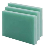
FR4 is a woven glass and epoxy laminate with a dielectric constant around 4.2 to 4.8 and a loss tangent near 0.02. It is inexpensive, widely available, mechanically strong and easy to process. The problem for high frequency work is not a single number but its variability. The dielectric constant of FR4 changes with frequency and with temperature, and different resin contents and glass weaves give different values, which makes precise impedance control harder. Its loss tangent is roughly ten times that of a typical PTFE based material, so insertion loss climbs quickly, and its moisture absorption shifts the electrical properties in humid conditions. FR4 remains an excellent choice for digital boards, power electronics and low frequency RF up to a few hundred megahertz.
High-Frequency Laminate Characteristics
High frequency materials are built to keep the electrical properties stable. Most are based on PTFE with a ceramic filler, or on hydrocarbon and thermoset systems, and they span a dielectric constant from about 2.2 up to 10 or more. The loss tangent is far lower, typically in the range of 0.0009 to 0.004 depending on the grade, and the dielectric constant varies little with frequency or temperature. That stability is what makes them valuable: a design can hold a 50 ohm line across a wide band, and the insertion loss budget can be predicted rather than guessed. The trade is cost, availability and a different set of processing requirements.
How the Stack-Up Itself Differs
Layer arrangement. High frequency designs put the RF layer immediately adjacent to a solid ground plane, and often keep the dielectric between them thin to tighten coupling and reduce radiation. Mixed stacks. A common and economical approach uses FR4 for the digital and power layers with one or two high frequency layers bonded in, so the expensive material is used only where the signal actually needs it. Ground planes. The reference plane has to be continuous under every RF trace, with via stitching along the edges of the RF region and around the antenna feed. Solder mask. Some RF designs remove solder mask over critical lines, because mask has its own dielectric constant and loss, while others specify a low loss mask. Symmetry. The stack still has to be balanced to control warpage, which can be harder with mixed materials that expand differently.

Impedance and Trace Width
Because the dielectric constant is lower, a 50 ohm microstrip on a high frequency laminate is wider than the same impedance on FR4 at the same dielectric thickness. This is often mistaken for a disadvantage, but the wider trace also lowers conductor loss and is easier to etch accurately. The practical point is that the trace geometry has to be recalculated whenever the material changes, and the fabricator has to build to the dielectric thickness that the calculation assumed. In a mixed stack, the geometry changes layer by layer, so the impedance targets must be listed per layer on the fabrication drawing rather than as a single global value.
Cost and Manufacturability
High frequency laminates cost several times more than FR4 per square metre and are available in fewer thicknesses and panel sizes. They also behave differently in the shop. PTFE based materials are soft, so they are prone to smearing during drilling and usually need plasma treatment to prepare the hole wall before plating, since they do not respond to permanganate desmear the way epoxy does. They also expand more with temperature, so drilling parameters and registration have to be adjusted. Lamination of a mixed stack requires careful control of the press profile because the two material classes flow differently. All of this adds process cost on top of the material cost.
Choosing a stack-up is a joint decision between the RF engineer and the fabricator, because the achievable geometry depends on the material the shop can actually process. Review how PCB manufacturing builds mixed and high frequency stacks, keep the RF rules in your PCB design and layout, and check the design and manufacturing considerations before release. A prototype PCB assembly run with a measured S parameter sweep confirms the stack before volume.
When to Switch
Stay with FR4 while the highest frequency of interest stays below a few hundred megahertz, the trace lengths are short and the loss budget is generous. Move to a high frequency material when the loss budget becomes tight, when the frequency climbs into the gigahertz range, when the dielectric constant has to be known and stable across temperature, or when a filter or antenna depends on a repeatable dielectric constant. Where only part of the board is RF, use a mixed stack and keep the expensive laminate to the layers that carry the critical signals, which usually delivers most of the performance at a fraction of the cost.
FAQ
Can FR4 be used for RF? Yes, up to a few hundred megahertz and for short runs, but loss and dielectric variability become limiting at higher frequencies.
Why is the loss tangent so important? It sets how much signal energy the laminate absorbs, which directly controls insertion loss and therefore link margin.
What is a mixed stack and why use it? It combines FR4 digital and power layers with one or two high frequency layers, so the specialty material is used only where it is needed.
Does PTFE need special processing? Yes. It is soft and chemically inert, so it requires tuned drilling and plasma treatment before plating.
Conclusion
FR4 and high frequency laminates differ in dielectric constant stability and in loss, and those two properties decide how a stack-up is arranged. FR4 covers digital, power and low frequency RF at low cost; high frequency material buys predictable impedance and low loss where the link budget is tight. Decide from the frequency and the loss budget, use a mixed stack where only part of the board is RF, and confirm the geometry with the fabricator in 2026 before the layout is frozen.