PCB Design and Manufacturing: Key Technical Considerations
Printed circuit boards (PCBs) are fundamental components of modern electronic products. The quality of PCB Design and PCB Manufacturing directly affects the electrical performance, stability, reliability, and service life of the final product.
From circuit architecture and component placement to material selection, fabrication, soldering, inspection, and testing, every stage requires careful engineering control. Understanding these key considerations helps engineers develop reliable circuit boards while reducing manufacturing risks and production costs.
Key Considerations in PCB Design
Circuit Design
Circuit design is the foundation of a reliable PCB. It determines the functionality and electrical performance of the entire electronic system.
During PCB Design, engineers need to consider component placement, signal routing, power distribution, grounding, signal integrity, and circuit topology. The board size, layer count, material structure, and electrical requirements should also be defined according to the product application.
For complex products, professional PCB Design Services can help integrate schematic review, PCB layout, stack-up design, impedance control, DFM analysis, and EMC considerations into the development process.
A well-designed PCB should not only satisfy the electrical requirements but also provide a practical foundation for subsequent manufacturing and assembly.
Component Selection
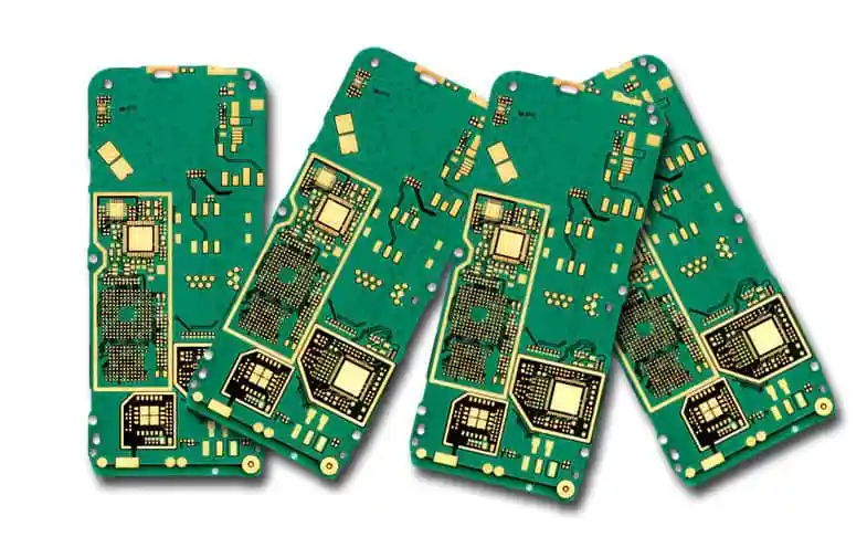
Component selection has a direct impact on PCB performance, reliability, and maintainability.
Engineers should evaluate electrical specifications, package type, operating temperature, reliability, availability, and compatibility when selecting components. The selected components should meet the functional requirements of the circuit while allowing sufficient flexibility for future maintenance and replacement.
Component placement should also take into account signal paths, thermal requirements, assembly processes, mechanical constraints, and accessibility.
Thermal Management
As electronic products become smaller and power density increases, thermal management has become an increasingly important part of PCB Design.
High-power components can generate significant heat during operation. If heat is not effectively dissipated, excessive temperatures may reduce component reliability and shorten product life.
Thermal design may involve optimized component placement, copper areas, thermal vias, heat sinks, metal-core structures, and appropriate PCB Materials.
For applications with demanding thermal requirements, PCB Manufacturing should be coordinated with the thermal design from the beginning so that material selection and fabrication capabilities match the application.
Electromagnetic Compatibility
Electromagnetic compatibility (EMC) refers to the ability of electronic equipment to operate properly in its electromagnetic environment without causing unacceptable interference to other devices.
During PCB Design, engineers should consider electromagnetic interference, signal coupling, return paths, grounding, shielding, filtering, and high-speed signal routing.
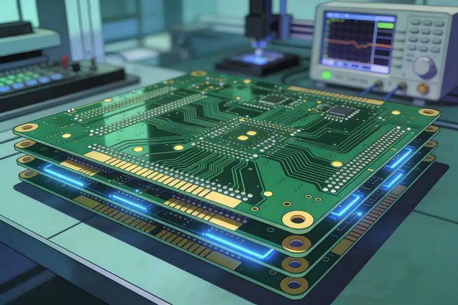
For multilayer boards, appropriate ground planes and controlled routing strategies can help reduce crosstalk and electromagnetic interference. High-speed circuits may also require controlled impedance and carefully engineered stack-up structures.
Key Considerations in PCB Manufacturing
Material Selection
Selecting appropriate PCB Materials is essential for achieving stable electrical, mechanical, and thermal performance.
Different applications may require different substrate characteristics. Standard FR-4 materials are widely used for general-purpose electronic products, while high-Tg materials may be appropriate for higher-temperature applications. High-frequency laminates, flexible materials, aluminum substrates, and other specialized materials may be selected according to electrical, thermal, mechanical, and environmental requirements.
Material selection should consider:
- Electrical performance
- Dielectric properties
- Thermal resistance
- Mechanical strength
- Operating temperature
- Environmental requirements
- Long-term reliability
- Manufacturing compatibility
The correct material should be selected according to the actual application rather than simply choosing the most advanced or expensive option.
Manufacturing Precision
Manufacturing precision has a direct influence on PCB reliability and electrical performance.
The PCB Fabrication Process typically involves multiple controlled stages, including inner-layer imaging, etching, lamination, drilling, copper plating, outer-layer processing, solder mask application, surface finishing, and electrical testing.
Manufacturers must maintain accurate control over board dimensions, trace width, spacing, hole sizes, layer registration, copper thickness, and other critical parameters.
For high-density and advanced PCBs, manufacturing accuracy becomes even more important because small dimensional deviations can affect impedance, via reliability, component assembly, and overall circuit performance.
Soldering and Assembly
Soldering is a critical stage in PCB assembly because it creates the electrical and mechanical connection between components and the circuit board.
Depending on the product design, manufacturers may use SMT, through-hole technology, or mixed assembly processes.
Soldering parameters must be properly controlled to ensure reliable connections while minimizing thermal stress and mechanical damage. Factors such as solder paste, reflow temperature profile, component package, pad design, and PCB surface finish can all influence soldering quality.
A reliable PCB Manufacturing process should therefore integrate PCB fabrication and assembly considerations rather than treating them as completely independent stages.
PCB Inspection and Testing
Electrical Testing
After PCB fabrication and assembly, electrical testing is used to verify whether the board meets the intended electrical requirements.
Depending on the product, testing may include continuity testing, insulation testing, flying probe testing, in-circuit testing, or functional testing.
Effective PCB Testing helps identify open circuits, short circuits, incorrect connections, and other electrical defects before the product reaches the customer.
Visual and Dimensional Inspection
Visual inspection and dimensional inspection are also important parts of quality control.
Typical inspection items include:
- Board dimensions
- Hole position and size
- Copper surface condition
- Solder mask quality
- Silkscreen clarity
- Surface finish
- Board warpage
- Component placement
- Solder joint quality
For complex products, inspection may be combined with AOI, X-ray inspection, and other automated or specialized methods.
A structured quality management system can further improve consistency throughout PCB fabrication and assembly. PCB Quality Management typically covers design review, DFM inspection, incoming material control, manufacturing, assembly, and testing.
Environmental and Reliability Testing
Some applications require additional environmental and reliability testing before a PCB can be approved for production.
Depending on the intended operating environment, tests may evaluate temperature resistance, humidity resistance, vibration, mechanical stress, thermal cycling, and other reliability factors.
These tests help determine whether the PCB can maintain stable performance throughout its expected service life.
Integrating PCB Design with Manufacturing
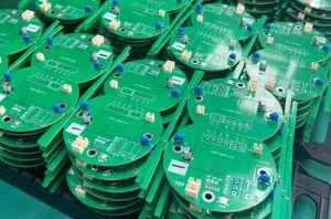
The most reliable approach is to consider design and manufacturing requirements together rather than treating them as separate stages.
A design that looks electrically correct may still create manufacturing difficulties if it uses impractical trace dimensions, insufficient spacing, complex via structures, unsuitable materials, or unnecessarily tight tolerances.
Design for Manufacturing (DFM) analysis can identify these potential problems before fabrication begins. Early engineering review can reduce redesigns, production delays, material waste, and manufacturing costs.
For projects requiring both fabrication and assembly, an integrated manufacturing partner can also coordinate PCB fabrication, component sourcing, SMT, through-hole assembly, inspection, and functional testing. One-Stop PCBA Services can simplify communication and improve process continuity from prototype development through production.
Conclusion
PCB development is a complex process that requires coordination between electrical design, materials engineering, manufacturing, assembly, and quality control.
A successful project begins with a robust PCB Design, continues with appropriate PCB Materials and a controlled PCB Fabrication Process, and ends with comprehensive PCB Testing and quality verification.
By integrating design requirements with manufacturing capabilities from the beginning, engineers can improve product reliability, reduce production risks, and create PCBs that consistently meet the electrical, mechanical, thermal, and environmental requirements of modern electronic products.
For projects ranging from prototypes to volume production, choosing a manufacturing partner with integrated design, fabrication, assembly, and testing capabilities can provide a more efficient path from concept to finished electronic product.