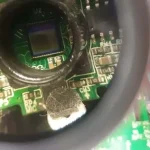
Solder Mask Slivers: Causes and Design Fixes
What a Sliver Is
A sliver is a narrow strip of solder mask that is not fully supported by the board surface, either because it is thinner than intended or because it sits between two openings that leave it barely attached. In its mild form it is a cosmetic defect that an inspector circles. In its serious form it lifts during reflow, breaks away and travels, or bridges two adjacent pads, and it becomes a functional defect: a short between two fine pitch pins, or a mask fragment sitting under a component where it prevents the solder from wetting. The mechanism is mechanical rather than chemical, and it is decided almost entirely by the geometry of the mask artwork and the registration achieved in production.
Where Slivers Come From
The common source is a mask dam that is narrower than the process can reproduce reliably. Between two fine pitch pads the mask strip is set by the pad pitch and the mask expansion, and if that strip comes out at a few tens of micrometres it is too fragile to survive the develop, cure and reflow steps. The second source is registration: a mask opening that is not perfectly centred on its pad leaves one side of the dam thinner than the other, and where the shift is large the dam nearly disappears on one side. The third is a mask opening that is too large relative to the pad, which is often a deliberate attempt to make soldering easier and which eats the dam width. The fourth is a design where the mask is asked to cover a step, a trace edge or a via that creates a thin unsupported shelf.
Design Rules That Prevent Them
The rule that matters most is the minimum mask dam width, which is a process number: ask the fabricator what the smallest reliable strip is, and design the pad pitch so that the resulting dam is at least that wide with the intended expansion. Where the pitch does not allow it, the alternatives are to reduce the expansion, to change the finish so that a mask defined pad is acceptable, or to accept a mask opening that spans two pads and rely on the solder volume and stencil design to prevent bridging. The second rule is to keep the expansion consistent and small, and to check it against the registration capability rather than against an old drawing. The third is to avoid unnecessary mask features: a lonely strip of mask between two large openings, a thin outline around a pad, or a decorative stripe is a defect waiting to happen and contributes nothing to the function.
Registration, Not Only Width
Even a generously wide dam fails if the registration is poor. Mask registration is the positional accuracy of the opening relative to the pad, and it is influenced by the imaging, the exposure, the development and the way the panel is supported. A process that holds a tight registration allows a narrower dam; a process with a looser registration requires a wider one, and the design should be made against the capability of the shop that will build it rather than against a general rule. Where the design has to run on more than one shop, the dam width should be set by the worst of them, or the design should be reviewed against each process before release.

Inspection and Disposition
Slivers are found by visual inspection and by automated optical inspection, and the two disagree more often on this defect than on most, because a sliver is a judgement about support rather than a measurement. A useful acceptance criterion is practical: if the mask strip is fully supported by the board and has not lifted after the thermal excursion of assembly, it is acceptable; if it is lifted, broken or missing, it is a defect. Because a lifted sliver can travel and create a short, the disposition of a board with a lifted sliver between two different nets should be conservative, while a lifted sliver in an area with no nearby conductor is a cosmetic issue. Where the defect recurs, the answer is a design change, not a tighter inspection.
When It Shows Up in Assembly
Some slivers survive fabrication and fail at reflow, because the thermal excursion and the flux chemistry attack the weak point. This is why the same board can pass incoming inspection and fail on the line, which makes the defect look like a process problem at the assembly house. The distinguishing evidence is that the mask fragments appear near the affected pads and the mask edge shows a tear rather than a cut. Where this pattern appears repeatedly, the correct response is to check the dam width and the registration on the delivered panels and then to change the design of the pads and the mask openings rather than to adjust the assembly profile.

FAQ
What is a solder mask sliver? A narrow strip of mask between two openings that is too thin or too poorly supported to survive processing, so it lifts, breaks away or fails to form.
What causes slivers? A dam narrower than the process can reproduce, poor mask registration, an excessive mask expansion and mask features that are not needed for any function.
How wide should a mask dam be? At least the minimum the fabricator can reproduce reliably, which is a process number, with the pad pitch and mask expansion set so the resulting dam meets it.
Can a sliver be repaired? A lifted sliver between two nets is a reject. Rework of mask is possible in some cases, but the reliability of the repair is lower than the original coating.
Why do slivers appear only at reflow? Because the thermal excursion and the flux attack the weak point of an unsupported strip, so a defect that survived fabrication can lift during assembly.
Conclusion
Slivers are a geometry problem, and the fix is in the pad pitch, the mask expansion and the dam width rather than in inspection. Ask the fabricator for the smallest reliable dam, design the pitch so the resulting strip meets it, keep the expansion consistent, remove mask features that serve no purpose, and treat a lifted sliver between two nets as a functional defect. The mask capability and the minimum dam width are part of PCB capabilities, the pad and mask geometry belongs in PCB design and layout, and the imaging and cure steps are described in PCB manufacturing. A prototype PCB assembly run is where an unsupported sliver lifts and becomes visible in 2026.