PCB Etching: Chemical Versus Laser Methods
Two Ways to Remove Copper
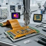
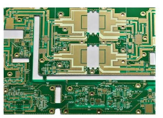
Etching is the step that turns a laminated copper sheet into conductors, and there are two practical ways to do it. Chemical etching dissolves unprotected copper in a bath, using a photoresist image as the mask. Laser etching removes copper thermally, by ablating it with a focused beam, either as the primary patterning method or to trim and clean features that chemical etching cannot reach. The two are not competing for the same job in most shops; they are used where each one is strongest.
Chemical Etching in Practice
The panel arrives with a resist image on both sides, and the etchant, usually an alkaline ammonia or a cupric chloride chemistry, is sprayed onto the surface from oscillating nozzles. The spray pressure, the conveyor speed, the temperature and the chemistry concentration are balanced so that the copper is removed at a controlled rate. Because the etchant works in every direction, it removes copper sideways under the resist as well as downwards, and that sideways attack is the defining characteristic of the process.
Etch Factor and Undercut
Etch factor is the ratio of the copper thickness removed to the sideways undercut, and it is the number that decides how fine a line a process can hold. A trace that is 100 micrometres wide at the top may be only 70 micrometres at the base after etching, and the trapezoidal cross section that results changes the impedance of the line. Thin copper etches to a better etch factor than thick copper, which is why fine-line layers are built on thin copper and why heavy copper layers cannot carry fine features. The designer’s protection is to specify the trace width as the finished width and to know which end of the trapezoid the fabricator is measuring.
Laser Etching and Ablation
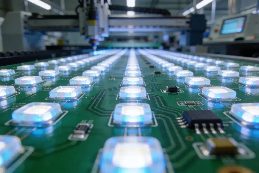
Laser processing removes copper without a wet bath, so there is no undercut and no etchant drag. The beam can produce a nearly vertical sidewall, and its positional accuracy is set by the motion system rather than by the chemistry. The trade is throughput and thickness: the process is slow per unit area, so it is normally used for small features, for trimming, for removing a thin copper layer or a plating seed, and for cutting fine patterns on materials where wet processing is difficult. Where a design needs a slot in copper, a fine isolation cut or a repaired feature, the laser is the tool. Where a design needs a whole layer patterned, chemical etching is the only economic answer.

Where Each Method Wins
Chemical etching wins on area, on cost per panel and on the ability to pattern an entire layer at once. Laser wins on precision, on vertical sidewalls, on the absence of undercut and on the ability to work selectively without masking the whole panel. A typical fine-line HDI build uses chemical etching for the pattern and laser processing for the microvias and for any local copper removal. A typical heavy-copper power board uses chemical etching with a generous etch factor and accepts that the features will be coarse.
Common Defects
The classic chemical defect is the open circuit caused by a pinhole in the resist, and its companion, the short caused by a scratch. Less obvious are the intermittent faults from thin copper, where a trace is etched to the point that its cross section will not carry the current, and the impedance error from a line that is much narrower at the base than the design assumed. Etchant drag, where the bath is depleted in a dense area, produces under-etched features that still show copper between traces. Laser processes have their own defects: a recast layer along the cut, heat-affected material, and a taper that depends on the beam focus.
Choosing for a Design
Decide the conductor width from the current and the impedance, then ask the fabricator what etch factor they hold on the copper thickness you have chosen. If the answer means the finished trace will be significantly narrower than the nominal, either reduce the copper thickness, widen the nominal, or move the layer to a laser-trimmed process. Keep the copper thickness on fine-line layers separate from the copper thickness on power layers, and remember that both live on the same board and must be built in the same sequence.
Inspection and Process Control
Both processes need their own control loop. In a wet line the etch rate drifts with the bath concentration, the temperature and the copper load on the panel, so the conveyor speed is adjusted against a periodically etched coupon rather than held at a fixed value. Automated optical inspection catches opens and shorts but cannot see a trace that is 30 percent thin, so thickness and width are checked by coupon or by cross section. In a laser process the control is the pulse energy, the focus position and the number of passes, and the useful check is a cut quality sample cut with the same recipe on the same material. Neither method can be verified after the fact from the finished product, which is the reason both rely on coupons and on statistical process control rather than on final inspection.
FAQ
What is etch factor? The ratio of the copper thickness etched to the sideways undercut, which sets how fine a line the process can hold.
Why is a trace narrower at the base? Because the etchant attacks sideways under the resist, producing a trapezoidal cross section rather than a rectangular one.
Is laser etching more accurate? Yes, it has no undercut and a nearly vertical wall, but it is much slower per unit area.
Can the two be combined? Routinely. Chemical etching patterns the layer and laser processing drills microvias or trims local features.
How does etching affect impedance? Through the trapezoid. The average width of the trace, not the drawn width, is what ends up in the impedance calculation.
Conclusion
Chemical etching trades precision for area, and laser processing trades speed for precision, so most boards use both. Specify trace widths as finished dimensions, ask what etch factor the fabricator holds on the copper thickness you have chosen, and keep fine-line and heavy-copper requirements on separate layers. Etch tolerances belong with PCB capabilities, the imaging and etching sequence is described in PCB manufacturing, and the widths and impedances that have to survive the process are set in PCB design and layout. Fine-line prototypes are normally verified through prototype PCB assembly in 2026.