Stepped Cavities and Depth Control in PCB
What a Stepped Cavity Is
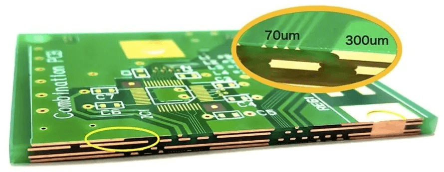
A stepped cavity is a recess milled into a board so that one area is thinner than the rest, without cutting all the way through. The result is a shelf at a controlled depth, used to sink a component into the board, to expose an inner-layer feature for a sensor or an antenna, to create a window in a rigid-flex stack so that the flex can fold inside the outline, or to provide a shoulder for a metal insert. The defining feature is that the cavity has a floor, and the depth of that floor relative to the surface is the number the fabricator has to hold.
How the Cavity Is Machined
Most cavities are produced by depth-controlled routing, where the milling bit is set to cut to a programmed Z depth rather than through the panel. The alternative is controlled-depth lamination, in which the cavity is formed by a prepared opening in the prepreg or the core, and the depth is set by the number of layers left in place. Lamination-formed cavities hold their depth better and give a cleaner floor, but they need a dedicated stack-up and a filler material to prevent resin flowing into the opening. Milled cavities are more flexible and can be added to a wide range of stacks, at the cost of a routed floor with tool marks and a depth tolerance that depends on the machine and on the flatness of the panel.
Depth Control and Tolerance
Two things make cavity depth difficult. The first is that the reference surface is not perfectly flat. Panel thickness varies across the sheet and after lamination, and a machine that measures depth from the surface will follow that variation into the cavity floor. The second is that the depth is usually set to leave a specific dielectric thickness between the floor and the next copper layer, so the tolerance on the remaining material is the number that matters for electrical performance rather than the cavity depth itself. A typical milled cavity holds depth to a few tens of micrometres, and the remaining dielectric under the floor should be specified with that tolerance in mind.
Zoning and the Fabrication Drawing
A stepped cavity has to be described on the fabrication drawing in a way that leaves nothing to interpretation. The drawing needs the cavity outline, its depth and the reference surface for that depth, the tolerance on the remaining dielectric beneath the floor, the copper features that must not be exposed or damaged, and the surface finish inside the cavity. Where the cavity is deeper than one layer, the layer at the floor should be identified by name. A cavity that is dimensioned only by its outline is a cavity whose depth will be guessed.
Rigid-Flex Windows and Depth
In rigid-flex work, the cavity is often used to remove the rigid material from an area so that the flex section can bend inside the board outline, and the depth control decides how much of the stack remains. Milling too deep removes the flex layers entirely and destroys the circuit; milling too shallow leaves rigid material that fights the bend and cracks the coverlay. The useful convention is to specify the cavity relative to the flex layers rather than to the outer surface, so that the fabricator knows which material must survive. The transition between the cavity and the flex region should be kept away from the bend line, because the step is a stress riser.
Design Rules
Keep the cavity walls away from fine traces by at least the routing tolerance plus a margin, since a wall that clips a trace is a short or an open. Avoid placing a cavity directly over a component that generates heat unless the remaining dielectric is thick enough to spread it. Do not design a cavity whose floor is thinner than the minimum dielectric the fabricator can control, and check the aspect of the cavity: a narrow, deep cavity is difficult to mill cleanly. Where a cavity will be exposed to the environment, specify the finish on the floor and consider moisture ingress. Finally, remember that a cavity interrupts the plane, so any controlled-impedance line that crosses the cavity changes its reference and must be rerouted or re-modelled.
Yield and Cost
Cavities are a yield risk because they are cut late in the process, after most of the value has been added. A milled cavity that goes too deep scraps a fully processed panel, and the depth control therefore has to be verified on a coupon or on a test area before production. Lamination-formed cavities reduce the risk to the milling step but add stack-up complexity and filler handling. Either way, the cost is driven by the depth tolerance requested: a looser tolerance allows a simple milled cavity, while a tight tolerance on the dielectric remaining beneath the floor pushes the shop toward a laminated construction.
Communication Between Design and Shop
Most cavity failures come from a drawing that leaves the geometry implicit rather than from a machine that cannot hold the tolerance. The fabrication note should say what the cavity is for, since a recess for a component, a window for a bend and an opening for a sensor have different priorities: a component recess needs a flat floor and a consistent remaining dielectric, a bend window needs the flex layers intact, and a sensor opening may need an exposed pad with a defined finish. Adding the purpose costs one line on the drawing and removes the most common source of a scrapped panel. Where the cavity interacts with plating or with a coating, the note should also state whether the cavity is milled before or after those steps, because the sequence changes the finish on the floor and the risk of contamination inside the recess.

FAQ
What is a stepped cavity? A controlled-depth recess in a board that leaves a shelf at a defined depth rather than cutting through the panel.
How is the depth controlled? By depth-controlled routing or by forming the opening in the prepreg and laminating around it.
Why is the depth tolerance so hard to hold? Because the reference surface itself varies across the panel, and the target is usually the dielectric remaining under the floor rather than the cavity depth.
What should the drawing specify? The outline, the depth, the reference surface, the tolerance on the remaining dielectric, the protected copper features and the finish inside the cavity.
Can a cavity cross a controlled-impedance line? Not without re-modelling, because the removed material changes the reference and therefore the impedance.
Conclusion
A stepped cavity is a controlled-depth feature, so it should be specified as one: outline, depth, reference surface and the dielectric that must remain. Use laminated construction where the depth tolerance is tight, keep the walls clear of fine features, and never route a controlled-impedance line across a cavity without re-checking it. Cavity and step capabilities are listed under PCB capabilities, the milling and lamination steps are described in PCB manufacturing, and the layer planning that a cavity disturbs is part of PCB design and layout. Rigid-flex builds with cavities are normally proven through flex PCB assembly in 2026.