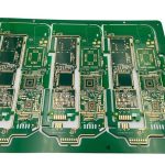
PCB Copper Wrap and Edge Plating Tolerance
What Copper Wrap Means
Copper wrap is the connection of a surface copper feature around the edge of the board to copper on another layer, so that the two are joined by metal that passes over or through the edge rather than by a via inside the outline. The most common uses are an edge connector where the pads must present copper on the side of the board, a shielding wall where a continuous ground plane has to reach the edge, and a castellation in a module where the edge is used as a solderable half-hole. In all three cases the requirement is the same: the copper must be continuous from the surface, around the edge, and it must survive the mechanical operations that shape the outline.
How the Wrap Is Formed
The usual sequence is to plate the board while the edge is still part of the panel, then profile it. Where the wrap is a simple surface-to-edge connection, the edge of the board is included in the plating pattern so that the barrel is continued around the profile. Where the wrap must connect two layers, the plating on the edge is deposited after the outline is formed in a second plating operation, or the board is built with the edge copper already patterned and then routed so that the plating is exposed. A castellation is a plated through-hole that is subsequently cut in half by the profile, which leaves a plated semicircular surface on the edge.
The Tolerance That Actually Matters
The number that matters is not the thickness of the copper on the edge but the continuity of the wrap, and the tolerance that governs it is the registration between the profile and the copper. Routing removes material along the outline with a tolerance of a few tens of micrometres, and the copper pattern has its own registration error, so the wrap has to be designed with enough overlap to survive both. Where the design leaves only a marginal overlap, a shift in either direction opens the connection or cuts it away. The practical rule is to specify the minimum width of the wrap as it appears on the finished edge, not the drawn width on the artwork, and to give the profile a clear area free of anything that a cutting tolerance would damage.
Edge Plating and Castellations
Edge plating is used for shielding and for connectors that clamp the board edge. It requires the plating to be continuous around the profile, which means the plating step has to follow the profiling step, and the edge surface has to be prepared so that the copper adheres. A castellation is a different structure with the same appearance: the hole is plated first, then cut, so the copper on the edge is the wall of a barrel rather than an electroplated film. The two have different mechanical behaviour, because a castellation is a solid plated barrel and an edge plating is a thin film on a machined surface. Where a module will be soldered onto a motherboard by its edge, the castellation is almost always the right structure, and it needs a specified half-hole diameter and a defined solderable depth.
Mechanical and Assembly Effects
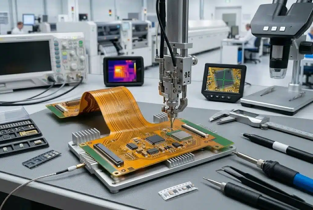
Copper on the edge is exposed to every handling operation, and it has no solder mask to protect it. An edge plating that is scraped during depanelling or during a fixture clamp can be damaged in a way that is not visible from the surface. Castellations are more robust, because the copper is supported by the laminate around the barrel, but they can still be torn if the tab that holds the board in the panel is placed across the castellation. Where the edge will be inserted into a connector, the plating thickness and the profile tolerance together determine whether the connector contact pressure is correct. Where the edge will be soldered, the finish on the edge determines solderability, and a finish that is applied only to the flat surfaces leaves the castellation unsolderable.
Design Rules That Avoid Trouble
Keep the edge copper, and the castellations, away from the breakaway tabs, so that depanelling does not cut through plated metal. Provide a mask keep-out on the edge. Specify the castellation diameter, the depth of the half hole and the remaining wall between neighbouring castellations, and check that the remaining laminate can carry the module weight. Do not place a castellation next to a high-current trace that would be exposed by the cut. Where the wrap is for shielding, verify that the connection is continuous around the whole outline, since a single interruption turns a shield into an antenna. Finally, agree with the fabricator which plating sequence will be used, because the achievable tolerance depends on whether the edge is plated before or after profiling.
Inspection and Acceptance
A wrap is inspected visually and by cross section. The visual check looks for continuity and for scratches, and a magnification check along the edge is usually enough to find a broken wrap. The cross section is what confirms the copper thickness on the edge and the overlap between the surface copper and the profile. Where the wrap is part of a shield, a continuity measurement around the outline is a more meaningful acceptance test than a visual one, because it tests the property that matters.

FAQ
What is copper wrap? Copper that connects a surface feature around the board edge to another layer, used for edge connectors, shielding walls and castellations.
What tolerance should I specify? The minimum wrap width on the finished edge, so that the profile tolerance and the copper registration error are both absorbed.
How is a castellation made? A plated through-hole that is cut in half by the profile, leaving a plated half-hole on the edge.
Is edge plating the same as a castellation? No. Edge plating is a thin plated film on a machined surface; a castellation is the plated wall of a drilled barrel.
Where do tabs go? Away from castellations and edge copper, so that depanelling does not tear the plated metal.
Conclusion
Copper wrap and castellations are edge features, so the tolerance that governs them is the relationship between the profile and the copper rather than the copper thickness alone. Specify the minimum finished wrap width, keep the tabs clear of plated edges, define the castellation geometry and the finish on the edge, and confirm the plating sequence with the fabricator before the data is released. Edge and castellation capability is described under PCB capabilities, the plating and profiling sequence belongs to PCB manufacturing, and the module layout that depends on it is part of PCB design and layout. Module assemblies of this kind are normally proven through PCB assembly in 2026.