BGA Signal Integrity: Fanout, Length Matching and Decoupling
A large BGA package compresses hundreds of connections into a few square centimetres, and it removes the ability to fix a routing problem along a trace. Everything that determines whether the high speed nets work is decided in the first few millimetres around the package: how the balls escape, how long the via barrels are, how the reference planes are arranged, and where the decoupling sits.
This article covers the four decisions that matter most, in the order they should be made, and the checks that catch each one before the layout is finished rather than after the first article is measured.
Fanout Sets the Electrical Environment
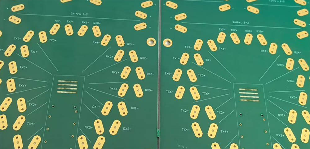
The escape pattern is not only a routing convenience. Each signal leaves the ball through a short top layer trace and then descends through a via, and each of those transitions is a change in impedance. If the escape segments differ in length, the impedance profile differs too, and the reflection at each transition varies from pin to pin. In a parallel bus that skews the edges of the group, which is exactly what the length matching later is trying to control.
Plan the fanout by function rather than by geometry. Power and ground balls normally sit around the periphery and in clusters beneath the die, and they should be taken straight to the planes to build the lowest possible impedance return for the signals beside them. The remaining pins are then grouped: data lanes, address and command, clocks and control, each escaping with similar geometry. Placing the via as close to the pad as the process allows is the single most effective way to reduce the stub that remains.
The Stub Is the Usual Cause of a Resonance
When a signal descends from the top layer to an inner layer, the unused part of the via barrel below the exit point behaves as an open stub. At low frequency that signal stub is invisible; as the edge rate rises it stops looking like a small discontinuity and starts looking like a resonator, and it produces a notch in the insertion loss at a frequency set by the stub length and the effective dielectric constant.
Every fanout via therefore carries a stub unless the barrel stops at the target layer. The remedy depends on how much room the escape has. If the layer being used sits close to the top, the stub is short enough to ignore. If the signal has to reach a deep layer, a blind or buried via that stops at the target layer removes the stub entirely, and a back drill operation removes the excess after plating. Both options cost money and both need to be agreed with the fabricator before the stack-up is fixed, because the drill capability defines what the stack-up is allowed to be.
Length Matching Is a Constraint With a Budget
A wide parallel interface, DDR being the familiar example, is matched within a group rather than across the whole bus. Data bits are matched to each other and to their strobe, the strobe is aligned to the middle of the data group, and the clock has its own tighter allowance. The numbers come from the controller and memory datasheets and from the timing budget of the interface, and they should be written into the design constraints before routing begins rather than checked afterwards.
Matching is implemented by adding length in serpentine sections, and the placement of those sections matters as much as the amount. Adding the compensation near the far end of the net, away from the package, keeps the dense region around the BGA free of long parallel detours. Inside the escape area, serpentine copper running side by side raises the coupling between adjacent nets, which can undo the timing benefit the matching was meant to deliver. Where the bus is dense, a ground trace between groups is a cheap way to lower the coupling, and the spacing between groups is a deliberate number rather than whatever is left over.

Decoupling Is a Placement Problem Before It Is a Selection Problem
A package with hundreds of supply balls needs a low impedance supply across a wide frequency range, and that is delivered by the planes first and the capacitors second. The useful pattern is a continuous power and ground plane pair beneath the package, capacitors placed around the periphery as close as possible to the supply balls they serve, and a mix of values so that the impedance stays low over the frequency band the device actually uses. A capacitor connected by a long thin trace has already lost most of its value at the frequencies where it is needed.
The stack-up is what makes all of this possible. Signals that need controlled impedance move to inner layers as microstrip or stripline, where the reference plane is defined and the environment is stable. The impedance of each layer is a function of trace width, copper thickness, dielectric thickness and dielectric constant, and the buried layer calculation also depends on where the reference planes are. For an interface running at the higher DDR rates, verifying the stack-up with a field solver or an impedance model is cheaper than discovering the error on a fabricated board, and the impedance test coupon on the production panel is what confirms the result afterwards.
Reviewing a BGA Design Before Release
Confirm the fanout pattern against the layer assignment as part of the layout review, then check the stub length on the deepest signals and decide whether the process needs a blind via or a back drill. Verify that the length constraints exist for every group and that the compensation sections sit in the permitted regions. Check the plane pairs under the package for continuity, and confirm that no dense via array has cut the reference into narrow necks. Finally, confirm the stack-up with the fabricator: the drill capability, the aspect ratio and the copper balance all constrain what the design can ask for, and those limits are cheaper to respect while the design is still a file. How the package is later mounted and inspected is covered in our assembly notes.
FAQ
Does every high speed signal need a blind via? No. The stub only becomes significant when its electrical length approaches a fraction of the edge rise time.
How tight should length matching be? As tight as the interface timing budget requires, and no tighter, because over-tight matching costs routing area and adds coupling.
Where should decoupling capacitors go? As close to the supply balls as the layout allows, connected to the planes rather than to long traces.
Can a two layer board carry a large BGA? Rarely with controlled impedance. A package of that density normally implies a multilayer stack-up.
Summary
BGA signal integrity is settled by decisions taken before any routing is finished: the escape pattern, the via structure and its stub, the length budget applied to the right groups, and a stack-up that puts the fast signals against a solid reference. Review those four against the actual device datasheets and the actual fabrication capability, and the measurements at first article become a confirmation rather than a diagnosis.