Through Hole Assembly and Wave Soldering Quality Control
Not every component can be placed on the surface. Connectors, terminal blocks, transformers, relays, large capacitors and anything that has to withstand a mechanical load are still mounted through the board, and the process that solders them is different from the one that forms a reflow joint. Through hole assembly introduces a second set of variables, and where both technologies appear on the same board the sequence in which they are performed becomes a design decision rather than a scheduling one.
Two Ways to Solder a Through Hole Joint
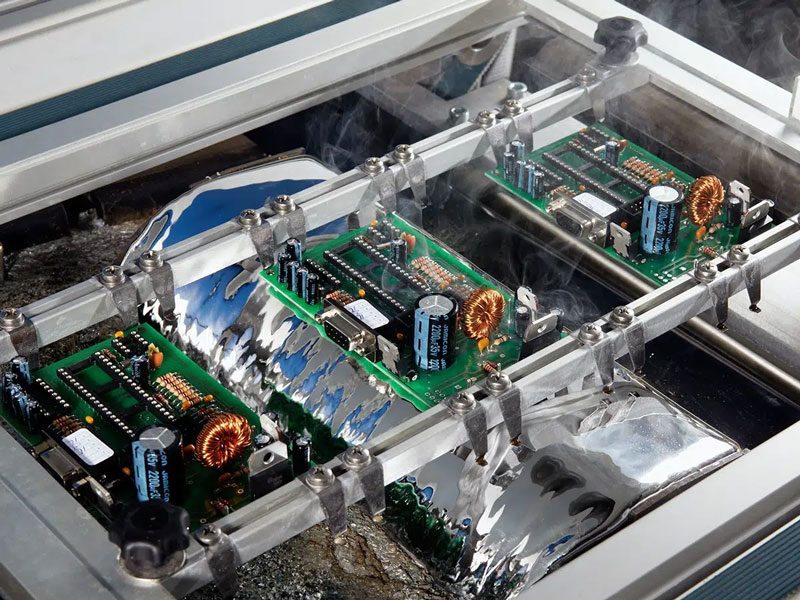
The traditional method passes the board across a wave of molten solder. The joints are formed simultaneously, which makes the process fast, and the wave reaches every through hole on the board, which makes it indiscriminate. Components that cannot tolerate immersion, boards with a high thermal mass and assemblies with fine pitch devices on the same side all constrain how the wave can be used.
The alternative is selective soldering, where a small nozzle delivers solder to one joint or one connector at a time. It is slower per joint and it allows the process to be tailored: the heat is applied where it is needed, the neighbouring surface mount devices are not exposed to the wave, and a connector with a large thermal mass can receive a longer dwell than one beside it. Where a board carries a small number of through hole parts among a dense surface mount population, selective soldering is often the only route that protects both.
Flux and Preheat
The flux is applied before the solder and its job is to remove the oxide from the pad, the lead and the molten alloy so that the metal surfaces can wet. The quantity and the placement matter: too little leaves an oxide film and produces a joint that looks formed but is not bonded, and too much leaves a residue that has to be cleaned and can trap moisture. The application method, whether sprayed, foamed or applied by a selective nozzle, determines how evenly the flux reaches the joints at different depths.
The preheat stage raises the assembly to a temperature at which the flux becomes active and the thermal shock of the solder is reduced. Its effect is easy to underestimate, because a board that is not preheated to a sufficient temperature will still produce joints, and those joints will be marginal in a way that only appears under thermal cycling. The preheat profile is measured on the actual assembly, using the same reasoning as a reflow profile: the board is not thermally uniform, and the heavy areas need more time than the light ones.
The Wave Parameters
The solder wave itself is characterised by its temperature, its contact time, its height and its shape. The temperature has to be above the liquidus of the alloy with enough margin to wet the joints, and low enough to stay inside the rating of every component on the board. The contact time is the product of the conveyor speed and the width of the wave, and it has to be long enough to fill the barrel and short enough to avoid damaging the laminate.
The wave height and shape determine how the solder reaches the joint. A wave that is too low leaves the joint unfilled; one that is too high floods the board. The flow of the wave affects the way the solder separates from the joint as the board leaves it, and a poor separation produces bridges between adjacent pins, which is the characteristic defect of the process.

Design Rules That Make the Process Reliable
The reliability of a wave soldered joint depends heavily on the design of the board. Thermal reliefs on the ground connections allow the pad to reach the soldering temperature without being drained by the surrounding copper plane. Adequate spacing between adjacent pins allows the solder to separate cleanly. A solder mask dam between the pads prevents a bridge from forming behind the pin. The orientation of the components relative to the direction of travel affects the shadowing, since a tall component can screen the joints behind it from the wave.
Where a board carries both technologies, the sequence is normally to reflow the surface mount devices first and to wave or selectively solder the through hole parts afterwards. The adhesive that holds the surface mount components in place, where it is used, the masking of areas that must not be soldered and the ability of the already soldered joints to survive a second thermal excursion are all decided at the design stage.
Inspecting and Correcting
A wave soldered joint is visible from the solder side, which means the inspection can be visual as well as electrical. The characteristics that matter are the fill of the barrel, the wetting angle at the pad and the lead, the presence of a fillet on both sides of the board and the absence of voids, bridges or icicles. A joint that is filled but not wetted looks acceptable at a glance and is the defect most often missed, which is why the inspection criterion is the shape of the fillet rather than the quantity of solder present.
Where a defect is found, the correction depends on its origin. A bridge is usually a wave or a spacing issue; an unfilled barrel is usually a preheat or a flux issue; a cold joint points to the thermal profile. Returning boards for touch up by hand resolves the individual symptom and leaves the process unchanged, which is why the investigation is aimed at the parameters rather than at the board. Our SMT assembly lines run both the reflow and the through hole processes, the mixed technology work is handled under mixed technology PCB assembly, the boards come from PCB manufacturing, the testing follows under PCBA testing and the records sit with quality management.
Why the Process Is Still Worth Getting Right
It is tempting to treat the through hole content of a board as a legacy problem, since the surface mount population covers the majority of the components and receives most of the process attention. The temptation should be resisted, because the through hole joints are frequently the ones that carry the mechanical load. A connector that has to accept a cable being pushed into it repeatedly, a terminal block that will have a wire tightened into it, a mounting point that will be bolted to a chassis, and a transformer that weighs more than the rest of the components combined are all mechanically loaded through their solder joints.
A joint of that kind fails differently from a joint on a logic device. It does not fail because the signal degrades; it fails because a crack propagates under a load that is applied thousands of times. The crack begins at a void, an unwetted area or a fillet with a sharp internal corner, and none of those is visible from a functional test that passes on the day the board is built. That is why the through hole process is inspected against a shape criterion rather than only against a continuity criterion.
The second reason is thermal. A barrel that is filled but porous carries current, and it carries it adequately in the short term. Under the thermal cycling of a real product, the difference between a sound barrel and a porous one becomes a difference in the rate at which the barrel cracks, and the product that fails in the field is the one whose process was accepted on the evidence of a bench test. Getting the preheat, the flux and the wave parameters right is what prevents that outcome, and it is cheaper than any inspection that could be applied afterwards.
FAQ
When is selective soldering preferred to a wave? When the board carries a small number of through hole parts beside dense surface mount devices that should not see the wave.
Why does a joint look formed but not bond? Usually because the flux was insufficient or the preheat too low, leaving an oxide film that prevented the alloy from wetting the pad.
What is the most common wave soldering defect? Bridging between adjacent pins, caused by the way the solder separates from the joint as the board leaves the wave.