




EMI Reduction Through Stackup and Layout Choices
Controlling emissions is usually discussed in terms of filters, chokes and shielding, all of which are applied to a finished design. The measures that decide the outcome, however, are taken before any of those components are considered. They are geometric: which layer a signal runs on, what sits beneath it, and where the current that returns from it flows. A stackup chosen for EMI reduction does more for a product than any filter that can be fitted afterwards.
Why the Stackup Is the First Control
A signal trace and its return current form a loop, and the field radiated by that loop grows with its area and with the rate of change of the current. Reducing the area is therefore the most direct way to reduce emissions, and the area is set by the distance between the trace and the plane beneath it. That distance is a property of the stackup, not of the routing.
This is why the standard recommendation places signal layers adjacent to ground planes. In a four-layer board, arranging the stack so that the two outer signal layers each have an inner ground plane beneath them gives every trace a return path within a few thousandths of an inch. The alternative arrangement, with the two signal layers adjacent to each other in the middle, leaves both without a close reference and produces a board that radiates far more for the same schematic.
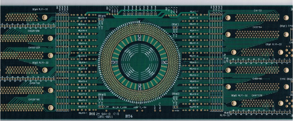
Where the budget allows, additional ground layers improve the situation further by dividing the board into shielded sections and by lowering the impedance of the return network. The arrangement of those layers is the subject of this article on layer stackup design.
Return Path Continuity
A return current follows the path of least impedance beneath the trace that generated it, which at high frequency means the plane directly under the signal. Anything that interrupts that plane forces the current to divert, and the diversion increases the loop area. This is the mechanism by which a split plane or a dense via field turns an otherwise quiet design into a radiator.
The practical rules follow directly. Do not route a fast signal across a plane split, and if a crossing is unavoidable, provide a stitching capacitor or a ground via adjacent to the crossing so the return has a short path. Keep the ground plane continuous beneath connectors and around the board perimeter. Where a signal changes layers, place a ground via next to the signal via so the return can change layers alongside it. The consequences of ignoring this are examined in this discussion of power plane splitting.
Layer Assignment for Fast Nets
Not every signal needs the same treatment. Clocks, fast serial links, switching supply nodes and any net with a sub-nanosecond edge belong on layers that are tightly referenced and, where possible, fully enclosed between planes. A stripline buried between two ground planes radiates almost nothing, because the field is contained within the dielectric. A microstrip on an outer layer radiates from the exposed side, though the amount is still small when the plane beneath is close.
Slow signals can be treated more loosely. Assigning the fast nets to the shielded layers and letting the slow control lines route on the outer layers is a cost-free optimisation, and it usually improves the layout as well because the fast nets are the ones with the simplest topology.
<img src="https://www.gopcba.com/wp-content/uploads/2026/08/eyJidWNrZXQiOiJ3ZXZvbHZlci1wcm9qZWN0LWltYWdlcyIsImtleSI6ImZyb2FsYS8xNzI5MTQ5MzQ5NDg1LUVOSUctMi5qcGVnIiwiZWRpdHMiOnsicmVzaXplIjp7IndpZHRoIjo5NTAsImZpdCI6ImNvdmVyIn19fQ.webp" alt="guard ring with vias placed around a noisy circuit block” />
Guard Rings and Local Shielding
A guard ring is a closed loop of ground copper placed around a noisy or sensitive circuit block, stitched to the ground plane with vias at intervals along its length. It works in two directions: it contains the field generated inside the ring and it prevents external field from reaching the circuit inside. The stitching is what makes it functional, because a ring grounded at only one point behaves as an antenna.
The spacing of the stitching vias sets the highest frequency at which the ring is effective. As a working rule, the spacing should be a small fraction of the wavelength at the highest frequency of interest, and in practice vias at intervals of a few millimetres around a small block are sufficient for most digital designs. The ring should be continuous, with no large gaps where the loop would be broken.
Local shielding beyond the ring is rarely necessary for a well-laid-out board, but where a specific component radiates strongly, a small shield can connected to ground at several points is more effective than a general shield over the whole assembly. The area covered by a shield should be limited to the region that requires it, because a large shield with a poor ground connection can make emissions worse.
Power Distribution and Decoupling
The power distribution network is an emissions path as well as a supply. Current drawn by switching devices returns through the ground network, and the loop it forms is a radiator. Decoupling capacitors placed next to the pins they serve confine that current to a small area, which is why placement matters more than the capacitance value in most cases.
The plane pair formed by a power plane and its adjacent ground plane also acts as a distributed capacitor, but it can resonate. The resonances appear as peaks in the emissions spectrum at particular frequencies, and they are controlled by keeping the planes closely spaced and by stitching them with vias at intervals. Where the board is large, the stitching should be regular rather than confined to the edges.
Reviewing the Layout for Emissions
Before the design is released, trace the return path of every fast net on the artwork and confirm that it is continuous and close to the signal. Check that no fast net crosses a plane boundary. Confirm that the ground planes are stitched with a regular via pattern and that no floating copper remains. Check that the guard rings around noisy blocks are complete and properly grounded.
Those four checks cost nothing and they address the mechanisms that dominate emissions below a few hundred megahertz. Where a design still fails an emissions test after them, the correction usually lies in the cable interface rather than in the board, and the coupling mechanisms involved are described in this discussion of EMI suppression design principles.
One further geometric rule deserves mention: keep copper away from the board edge. A plane that extends to the profile exposes its cross-section, and the fringing field at that edge radiates. Insetting the power plane relative to the ground plane by a distance related to the dielectric thickness is the standard remedy, and the clearance rules that apply at the edge are discussed in this article on via to trace clearance.
FAQ
Which stackup arrangement best reduces emissions? One in which every signal layer is adjacent to a ground plane, with the planes as close to the signals as the process allows. Beyond four layers, additional ground planes and a tighter arrangement of the plane pair give further improvement by lowering the return impedance and dividing the board into shielded sections.
How effective is a guard ring? It is effective when it is a continuous loop stitched to the ground plane at regular intervals. The effectiveness depends on the via spacing relative to the wavelength, so denser stitching extends the ring usefulness to higher frequencies. A ring grounded at one point is worse than nothing.
Can emissions be fixed after the board is built? Only within limits. Filters and shields can reduce what leaves through cables, and a small shield over a specific component can help, but a design whose return paths are broken will radiate from the board itself, and that cannot be corrected without changing the layout.


2 Comments
Ultra-High-Speed AI Board Design and Fabrication Guide
[…] by tens of degrees. The stackup question here overlaps with the general trade-offs described in EMI reduction through stackup and layout, because plane spacing serves both heat and […]
AI Mainboard PCB Design and Fabrication Guide
[…] dielectric between the power and ground planes supplies the highest-frequency current locally, and EMI reduction through stackup and layout starts from the same plane pair. Simulation of the power delivery network from DC to a few hundred […]