




Layer Stackup Design: One Layer to Eight Layers
The stackup is the foundation of the whole design and the one decision that cannot be repaired later. A routing mistake can be fixed with a patch or a rework, an impedance error can sometimes be trimmed with a resistor, but a board built on a poor stack will have EMC problems that no amount of layout effort will remove. Two rules govern the design of any stack, and they apply at every layer count.
Every signal layer must have an adjacent reference plane, either power or ground. And the main power plane and the ground plane must sit as close together as the process allows, so that the pair provides a useful coupling capacitance. Everything else is an arrangement of those two constraints.
Single Layer and Double Sided Boards
A single layer board has no plane at all, so signal return currents flow through whatever copper happens to be available, usually a sparse network of traces. Routing on such boards should be slow, low-frequency and untroubled by impedance. There is no reference plane to maintain, no controlled impedance and no meaningful return path planning, which makes the format suitable for simple power supplies and appliances rather than for anything digital at speed.
A double sided board is the first format where a plane becomes possible. The usual approach is to devote one entire side to a ground plane and route all signals on the other. This gives every trace a reference directly beneath it, which halves loop area compared with an unrouted return and dramatically improves EMC performance at almost no cost. The ground plane should be unbroken wherever possible, and the designer should resist the temptation to cut it for a convenience route on the plane side. The routing on such a board also needs generous spacing, because there is no plane to provide a return path beneath a trace and any fast edge will couple into whatever copper lies nearby. Where a design must pass an EMC test on the first attempt, the stackup decision should be made before the schematic is finished rather than after the layout is complete.
Four Layer Boards
The classic four-layer stack is signal, ground, power, signal. The two inner layers are planes, one of them ground and one of them power, and they are separated by the thinnest dielectric the fabricator can make reliable. That thin separation is what gives the pair its capacitance, and it also gives the outer signal layers a tight reference, so trace widths for a given impedance are small and routing is easy.
The alternative arrangement, signal, signal, power, ground, is sometimes chosen because it puts two routing layers adjacent to each other. It costs more than it saves. The two inner signal layers have no immediate reference, the outer layers reference planes that are further away, and the result is a board that radiates more and is harder to constrain. In most cases the first arrangement is the better choice.
Six Layer Boards
At six layers there is enough room to give each signal layer a close reference and to keep the power and ground planes adjacent. A common and effective arrangement is signal, ground, signal, power, ground, signal. Every signal layer touches a plane, the power plane sits between two grounds, and the tightest dielectrics are reserved for the plane pair and the critical signal layers.
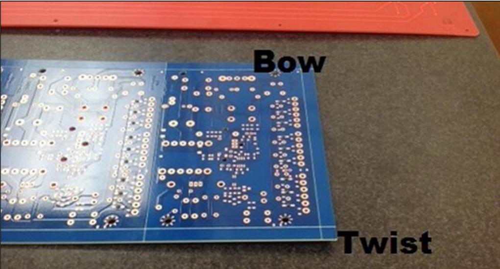
Symmetry matters at this layer count. A stack that is asymmetric will warp during lamination, because the copper distribution and the dielectric thicknesses differ between the two halves. Warpage affects drilling registration and therefore affects the clearance between holes and copper, a subject examined in this discussion of via to trace clearance on multilayer boards.
<img src="https://www.gopcba.com/wp-content/uploads/2026/08/led-pcb.webp" alt="power plane spacing measured between copper and reference layer” />
Eight Layer Boards and Above
An eight-layer board typically uses signal, ground, signal, power, ground, signal, ground, signal. This arrangement keeps the high-speed signals on layers that reference ground rather than power, which is preferable because a ground reference is continuous while a power plane is usually divided. It also provides two separate ground planes, allowing sensitive analog sections to reference their own plane without sharing return currents with digital circuitry.
The general principle at higher layer counts is that ground planes should be more numerous than power planes, and that the layers carrying the fastest signals should sit closest to a solid ground. Designers should also avoid placing two signal layers adjacent to each other, since neither can then reference a plane and both will have poor impedance control.
Controlled Impedance and the Microstrip Question
Once a stack is defined, the trace geometry follows. A trace on an outer layer over a plane is a microstrip, and its impedance is set by the trace width, the copper thickness and the dielectric height beneath it. A trace buried between two planes is a stripline, and its impedance is set by the trace width, the copper thickness and the distance to both planes. Because the dielectric heights are fixed by the stack, the designer’s only free variables are width and copper thickness.
This is why the stack should be agreed with the fabricator before routing begins, and why the fabricator’s actual material thicknesses matter more than the nominal values in a textbook. A 50 ohm microstrip on a 4 mil dielectric is a different width from a 50 ohm microstrip on a 6 mil dielectric, and a design that uses the wrong height will miss its target impedance by a wide margin. The same principle determines how far the plane must be inset at the board edge to control edge radiation and power plane splitting effects.
Practical Checks Before Release
Verify that every signal layer has an adjacent plane and that the layer directly beneath a fast signal is not a divided power plane. Confirm that the power and ground pair uses the thinnest available dielectric and that the stack is balanced in both copper and dielectric. Check that the impedance targets map to widths the fabricator can actually etch, and that the finished board thickness is available from the chosen material.
A stack that satisfies those checks will behave predictably, and predictable behaviour is what makes the difference between a design that passes EMC testing on the first attempt and one that requires a re-spin. Where a high-speed digital bus must be routed across the stack, the delay matching techniques described in this article on high frequency traces and data buses should be applied on the layers chosen here.
FAQ
Do I really need a plane on a four-layer board? Yes. The main benefit of four layers over two is that the inner layers can be dedicated to a ground and a power plane, giving every signal a reference. A four-layer board used as four routing layers has almost none of that advantage and costs the same to build.
Why should the power and ground planes be close together? The close spacing creates the distributed capacitance that supplies transient current to the devices on the board and keeps the power distribution impedance low at high frequency. A thin dielectric between the pair also lets the surface traces be narrower for a given impedance.
How do I choose between microstrip and stripline? Microstrip on an outer layer is easier to route and to adjust, and it is the usual choice for most signals. Stripline is fully enclosed by planes, so it radiates less and is immune to external coupling, which suits very fast or very sensitive nets. The choice depends on how much shielding the signal needs.



5 Comments
The 3W Rule: Trace Spacing for Crosstalk Control - Kingda
[…] rules and not the other way round. A design whose layer arrangement is described in this article on layer stackup design has already determined how much crosstalk a given spacing will […]
STM32 Core Board PCB Design Rules
[…] the digital one. The general rules that govern those arrangements are set out in this article on layer stackup design, and they apply to a core board exactly as they apply to a larger […]
Blind Via and Buried Via Stack Selection
[…] Because the via structures determine the lamination cycles, they must be decided with the fabricator before the layout is finished, not after. A designer who routes a dense board with through vias and only then discovers that blind vias are required has to restart the routing, since the escape patterns are different. The stackup itself should be agreed at the same time, using the principles described in this article on layer stackup design. […]
EMI Reduction by Stackup and Layout
[…] Where the budget allows, additional ground layers improve the situation further by dividing the board into shielded sections and by lowering the impedance of the return network. The arrangement of those layers is the subject of this article on layer stackup design. […]
PCB Routing: Microstrip and Stripline
[…] A stripline is a trace buried between two reference planes, so it is enclosed by copper on both sides. That enclosure gives it two advantages. The field is contained within the dielectric, so the trace radiates very little and is correspondingly immune to external coupling. And the impedance is determined by the geometry to both planes, which makes it more stable with respect to the manufacturing tolerances than a microstrip, whose impedance varies with the solder mask covering it. The general rules governing which layer a signal should occupy are described in this article on layer stackup design. […]