
Electroplating Via Filling Process for HDI Boards
As devices became denser, the holes that connect their layers became smaller, and once a hole is small enough that conventional plating cannot coat its walls uniformly, the process has to change. Instead of coating the barrel, the hole is filled completely with copper, so that the result is a solid column rather than a plated tube. The technique is called via filling, and it is what makes the highest-density boards possible.
Why Filling Rather Than Coating
A plated barrel has a wall of copper of finite thickness, and the thickness at the middle of the hole is always less than at the surface because the electrolyte is less accessible there. As the hole gets deeper relative to its diameter, the difference grows, and beyond a certain aspect ratio the coating in the middle becomes unreliable. The chemical and electrolytic plating combination used for conventional multilayer boards reaches its limit at that point.
Filling sidesteps the problem by depositing copper until the hole is closed. The result has no thin section, no void along the axis and no barrel to crack. It also produces a flat surface above the hole, which allows a pad or another via to be placed directly on top, and that is what makes stacked microvias structurally possible.
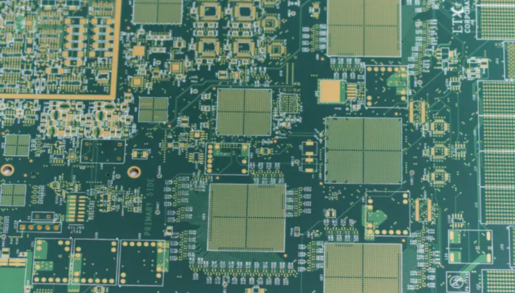
Chemistry and the Role of Additives
Filling is achieved with an additive system rather than with a single brightener. The electrolyte contains a suppressor that adsorbs on the surface and slows deposition, an accelerator that concentrates inside the hole and speeds it up, and a leveller that moderates the deposit at the surface. The combination produces the counter-intuitive result that the copper grows faster at the bottom of a small hole than on the flat surface around it, so the hole closes from the inside out.
The balance between those additives is what the process depends on. Too much suppressor and the hole plates slowly and incompletely; too little and the deposit builds on the surface instead of in the hole, producing a dimple or a void. The behaviour of these additives is described in more detail in this article on electroplating additives.
Where the Process Is Used
The principal application is in HDI constructions, where the holes are formed by laser and have a diameter measured in tens of micrometres. A blind via that must be filled has a small aspect ratio and a high surface area to volume ratio, and those proportions are what make the additive-driven filling mechanism work reliably.
Conventional mechanical holes in the same board are not filled, because they are too deep and too large for the process to close economically. The two hole types are handled in sequence, with the microvias filled and planarised before the mechanical holes are drilled. The overall sequence of an HDI build, including the laser drilling and the lamination cycles, is described in this discussion of HDI board CAM methods.
<img src="https://www.gopcba.com/wp-content/uploads/2026/08/copper-clad-plate-cutting.jpg" alt="copper plating inside a blind microvia during via filling” />
Defects That Appear When the Process Drifts
A filled via that does not close completely leaves a dimple in the surface. If a component pad or another via sits on top, the dimple becomes a void in the assembly or a discontinuity in the connection. A filled via that is over-plated leaves a bump, which interferes with the planarisation step and can cause a short where the copper is subsequently etched.
Voids inside the fill are the most serious defect, because they are invisible from the surface. They form when the deposition rate at the bottom of the hole outpaces the replenishment of the electrolyte, or when the additives are out of balance, and they show up as an open or a high-resistance connection after assembly. Detection is normally by cross-sectioning a sample from each panel rather than by inspecting every hole.
Cracking is the other failure mode. Copper filled into a small hole is subject to stress, particularly where the fill meets the target pad, and thermal cycling can open a crack at that interface. Controlling the plating stress and the annealing conditions is how the fabricator manages this, and it is one of the reasons a filled structure is not automatically more reliable than a plated one unless the process is well controlled.
Design Considerations
Where filled vias are used, the pad above the fill must be large enough to cover it with margin, since the fill surface is not perfectly flat. Where a component pad sits directly over a fill, the pad must be finished and planarised so that the paste does not drain into any residual depression; that combination is described in this article on via in pad and plated through holes.
The design should also keep the aspect ratio of the filled holes within the process capability, since filling a deeper hole is more difficult and more prone to voids than filling a shallow one. And where a stack of filled vias is used to connect several layers, each stage should be planarised before the next is added, or the accumulated surface irregularity becomes a yield problem.
Inspection and Process Control
Because the critical defect inside a filled via cannot be seen, the process is monitored rather than inspected. Samples are taken from production panels and cross-sectioned so that the fill profile, the presence of voids and the thickness of the copper above the target pad can be measured directly. The measurements are compared with the specification, and the additive concentrations in the bath are adjusted in response rather than on a fixed schedule.
The plating bath also requires continuous analysis because the additives are consumed at different rates. A suppressor is consumed by adsorption on the plated surface, an accelerator is consumed inside the holes, and the balance between them drifts as production continues. Platers use titration and electrochemical analysis to track the concentration and to dose the bath, which is why a filling process cannot be run from a fixed recipe alone.
The substrate contributes to the result as well. Resin residue left in the bottom of a laser-drilled microvia after the desmear step blocks the connection and prevents the fill from reaching the target pad, producing a high-resistance joint that passes a simple continuity test. Cleaning the hole properly before plating is therefore as important as the plating chemistry, and the interaction between the two is one reason HDI processes have a narrower window than conventional ones.
FAQ
Why is a via filled instead of plated? Because a plated barrel becomes thin in the middle as the aspect ratio rises, and beyond a certain ratio the coating is unreliable. Filling closes the hole completely, producing a solid connection with no thin section and a flat surface above it.
How does the copper grow inside a small hole? Through an additive system in which a suppressor slows deposition on the surface, an accelerator concentrates inside the hole and speeds it up, and a leveller moderates the surface deposit. The result is faster growth at the bottom of the hole than on the surrounding surface.
What is the most serious defect in a filled via? A void inside the fill. It cannot be seen from the surface and appears as an open or a high-resistance connection after assembly, which is why the process is monitored by cross-sectioning samples from production panels.