Via in Pad or Plated Through: Choosing by Cost
Placing a via directly in a component pad is a technique that solves a real problem and creates a real cost. It shortens the connection from a fine-pitch device to the inner layers and it frees routing space on the surface, both of which matter when the pitch is 0.5 millimetres or smaller. What it also does is add process steps that a normal plated hole does not require, and those steps are the reason a design should use the technique only where it earns its place.
What the Technique Does
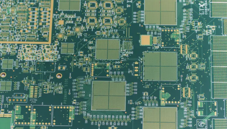
A conventional via sits beside the pad, connected by a short trace. That trace occupies surface area, and at fine pitch there may be no room for it. A via in pad puts the hole inside the pad itself, so the connection is direct and the trace disappears. The signal path is shorter, which reduces the parasitic inductance of the connection, and the surface area that the trace would have occupied is released for other nets.
For a ball grid array with a dense ball map, the technique is often the only way to route the device at all. The alternatives are a larger package, a higher layer count, or a via structure that costs more than the plugging process it was meant to avoid. In that context the additional processing is not a luxury; it is the enabler.
Why It Costs More
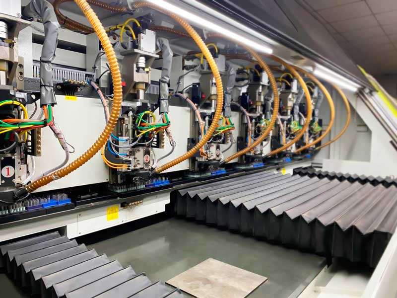
The added cost comes from the sequence of operations that a via in pad requires. The hole is drilled and plated like any other, but it must then be filled with a non-conductive resin so that the pad presents a flat surface. The resin is cured, ground back so that it sits flush with the copper, and the surface is planarised. After that, the pad is plated or finished along with the rest of the board, and the remaining holes are drilled and plated in the normal way.
Each of those steps carries its own yield risk. Resin that is not fully cured shrinks or outgasses during assembly. Resin that is not perfectly planar leaves a dimple in the pad, which produces a void in the solder joint underneath the ball. Grinding that goes slightly too far removes copper from the pad, which reduces the annular ring or exposes the resin. The process is well established, but it is less forgiving than a simple plated hole, and the cost reflects that.
The plugging and planarisation steps also interact with the geometry of the pad itself, since the solderable area that remains after planarisation is smaller than the pad as drawn. The implications for the joint are the same as any other pad geometry question, and the dimensional rules are set out in this article on PCB pad design standards.
When a Normal Via Is Enough
The first question to ask is whether the signal actually benefits. At low frequency, a short connection from a via beside the pad behaves almost identically to a via in the pad. The inductance difference matters at high frequency or for a power connection carrying fast transient current, and for a low-speed logic net the extra processing buys nothing that can be measured.
The second question is whether the routing is genuinely blocked. A design that uses vias in pads simply because they are available, rather than because the escape requires them, pays the cost without receiving the benefit. The escape routing analysis described in this discussion of escape routing and pad fanout answers that question directly: if the pads and traces fit without the technique, the design does not need it.
<img src="https://www.gopcba.com/wp-content/uploads/2026/08/8.jpeg" alt="resin plugging and planarisation steps for a via in pad” />
Partial Adoption
The usual answer is to apply the technique selectively. A design may need vias in pads only under the processor and only on the inner rows of balls, where the escape is hardest. The rest of the board can use ordinary vias at no additional cost. Because the plugging process is applied to specific locations rather than the whole panel, the cost scales with the number of holes rather than with the size of the board.
The same reasoning applies to layer count. Where the congestion that forces the technique comes from a shortage of routing layers, adding a layer may be cheaper than plugging several hundred holes. The decision is a comparison between two costs, and the comparison should be made with quotations rather than with assumptions.
Process Constraints
Where the technique is used, several constraints have to be respected. The aspect ratio of the hole must be within the plating capability, since the resin fill also becomes difficult in a deep narrow hole. The hole must be placed so that the remaining pad area is sufficient for the solder joint, which usually means that the pad must be enlarged relative to a conventional design. And the drill size should be as small as the process allows, because the resin fill and planarisation become easier as the hole gets smaller.
These constraints interact with the clearance rules around the hole and the pad, which are described in this discussion of via to trace clearance, and with the choice of via structure itself, which is the subject of this article on blind via and buried via stack selection.
Cost Optimisation in Practice
`r`n
Cost optimisation on a dense board is rarely a single decision. It is a comparison between the price of the extra process steps and the price of everything that would be needed to avoid them: additional layers, a different via structure, a larger package or a slower interface. Each of those alternatives has its own schedule impact as well, and a design that adds a layer to avoid plugging may gain a week of schedule while spending more on material.
`r`n
The useful discipline is to keep the technique confined to the locations that require it and to record which those are. A design that plugs two hundred holes deliberately is easier to quote, to review and to build than one that plugs two thousand because the option was enabled globally.
`r`n
Making the Decision
The decision procedure is short. Confirm that the routing cannot be completed without the technique, or that the electrical requirement genuinely benefits from it. Count how many holes actually need it. Obtain quotations for the design with and without, and for the alternative of an additional layer. Choose the option that satisfies the requirement at the lowest total cost, and record the reasoning so that the decision is not revisited without a reason.
FAQ
Why does a via in pad cost more than a normal via? Because the hole must be filled with resin, the resin cured, and the surface ground back flush with the copper before the pad is finished. Those steps add operations, equipment time and yield risk compared with a simple plated hole.
Can a via in pad be left unfilled? Not for a pad that must be soldered. An open hole in a solder pad allows the paste to drain into the barrel during reflow, which starves the joint and creates voids. The fill is what makes the pad a pad.
Is it cheaper to add a layer instead? Sometimes. Where the congestion that forces the technique comes from a shortage of routing layers, an additional layer may cost less than plugging several hundred holes. The comparison should be made with actual quotations rather than with assumptions about either cost.