PCB Circuit Board Design Steps: Requirements to Production Files
A circuit board that works on the first prototype is not the product of a single clever decision. It is the result of a sequence of steps, each of which narrows the options available to the next. Skipping a step does not remove the work, it moves the work to a later stage where it costs more. The sequence below is the one that has proven most reliable for boards ranging from a two-layer sensor module to an eight-layer controller, and each stage includes the checks that keep it from leaking into the next one.
Requirements and Circuit Design
PCB circuit board design starts with a written statement of what the board must do: the functional blocks it carries, the supply rails and their current, the interfaces it exposes, the environmental range it must survive, and the enclosure it has to fit. This sounds trivial until a board is laid out around an assumption that was never confirmed. The circuit design follows, expressed first as a block diagram and then as a schematic. The schematic should be reviewed for net naming, pull-up and pull-down values, and the placement of series elements before any physical layout begins.
Board Size and Layer Count
Board outline and stackup are decided early because both constrain everything else. The outline is usually set by the enclosure and the mounting hardware, leaving the designer to decide how much board area the circuitry actually needs. The layer count follows from the routing density and from the requirement for a continuous reference plane. A design with a single ground plane and modest density is well served by four layers, while a board with several controlled-impedance buses and multiple supplies will usually need six or eight. The trade-offs behind that decision are set out in this article on layer stackup from one to eight layers.

Component Selection and Schematic Design
Component selection is a design activity, not a purchasing one. A part with a long lead time can delay a project more than a marginal performance difference is worth, and a part available only in a package the assembly house cannot place is not usable at all. Where a choice exists, prefer standard packages, common values and parts with more than one source. During schematic design it is worth checking that every net has a defined state at power-up, that unused inputs are not left floating, and that the supply pins of each device are decoupled in the drawing as well as on the board.
Placement and Routing
Placement converts the schematic into a physical arrangement. Connectors and mechanical parts are fixed first, followed by the main device and its power section, then the analog and clock groups, and finally the passives that support what is already placed. Routing then proceeds from the most constrained nets to the least. The fastest nets, the differential pairs and the wide power paths are routed first because they have the least freedom; the general-purpose signals fill in around them. Keeping the return path of each fast net continuous is the single rule that most often decides whether the board passes emissions testing.
Ground and Power Planes
A dedicated ground plane is the reference for every signal on the board and the return path for every current. A power plane serves the same purpose for distribution, and the two should be adjacent where the stackup allows it so that the plane pair provides high-frequency decoupling. Splitting planes is sometimes necessary when a board carries isolated or quiet sections, but each split needs a clear rule about where signals may cross it, and crossing a split with a fast net is almost always a mistake. The reasoning behind those choices is covered in this article on power plane splitting rules.

Design Rule Check and Manufacturing Output
Before any file leaves the design office, the board should be run through a design rule check against the capability of the fabricator that will build it. Trace and space minimums, via drill sizes and annular rings, solder mask clearance and silkscreen line width are all checked at this point, along with connectivity and netlist agreement. The output package normally contains Gerber or ODB++ data, a drill file, a stackup drawing, a bill of materials and an assembly drawing. Missing information at this stage becomes an engineering question from the fab house, which costs a day each time it happens.
Prototype Build, Test and Revision
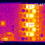
The first prototype has one job: to find the problems that simulation could not. Power rails should be checked under load before any device is expected to run, and the board should be exercised at the temperature extremes it was specified for. Signal integrity measurements on the fastest nets will show whether the routing met its impedance target, while thermal images will show whether heat is leaving the devices as intended. Any change that comes out of this stage should be reviewed against the same rules as the original design, since a late change is where new errors are introduced.
Cost, Documentation and Handover
Cost control is a design activity as well. Standard panel sizes, common materials, fewer layer counts and standard feature sizes all reduce price before a single unit is built. Documentation matters for the same reason: a revision that cannot be understood six months later is a revision that will be repeated. At gopcb the design package is treated as a deliverable in its own right, and the transition from design to fabrication is covered in this article on PCB design and fabrication. Thermal management decisions in particular should be recorded, because they are the hardest to reconstruct later.
Connectivity, Netlist and Documentation Checks
The netlist comparison is the last mechanical check before release, and it is the one that catches a change made after the final review. Comparing the copper connectivity against the schematic should be done on the frozen database, and every difference should be explained rather than waived. Documentation belongs in the same pass. A schematic with revision notes, a stackup drawing with material and thickness, an assembly drawing that shows orientation, and a list of the nets that were deliberately left unmatched will save more time during bring-up than any other hour spent on the board. It also makes the next revision of the same product a smaller task, since the intent behind each decision is recorded where the next engineer will look for it.
FAQ
How many design iterations should be planned for? One prototype round is normal for a straightforward board, and two for a board with controlled-impedance interfaces or tight thermal limits. Budgeting for zero iterations is what usually causes schedule overruns, and a schedule that assumes no rework leaves no room to absorb a fabricator query or a component substitution either.
Can routing start before the schematic is finished? Partially. The mechanical and power sections can be placed early, but routing fast nets before the netlist is frozen creates rework that is larger than the time saved.
Who decides the layer count, the designer or the fabricator? The designer decides it from the routing and return path requirements, and then confirms that the fabricator can build that stackup at an acceptable price.