PCB Design and PCB Fabrication Working Together
Design and fabrication are usually described as consecutive steps, as though the designer finishes and the fabricator begins. In practice they are a loop. The design determines what the fabricator has to achieve, and the fabricator”s capability determines what the design can ask for. Projects that treat the two as independent tend to discover the relationship late, in the form of a quotation that exceeds the budget or a board that fails inspection.
What the Design Side Produces
PCB fabrication begins with data that only the design side can produce, and schematic capture is the first of those products. Design starts with the circuit. The schematic is produced first, expressing the logical connections between components without reference to their physical positions, and it is verified before the layout begins because an error at this stage propagates into everything downstream. The netlist generated from the schematic is the contract between the two stages.
Layout then turns the netlist into copper. Placement positions the components against the mechanical constraints, the thermal requirements and the electrical grouping. Routing connects them, subject to the impedance, spacing and clearance rules that the electrical design and the fabrication process impose. The output of this stage is the artwork, and its accuracy depends on the component library being correct, since a footprint error becomes a manufacturing defect. The rules a footprint must satisfy are described in this article on PCB pad design standards.

What the Fabricator Needs
Fabrication needs more than the artwork. It needs the layer stack, with the material, the dielectric thicknesses and the copper weight for each layer. It needs the finished board thickness and the tolerance. It needs the surface finish, which affects solderability and shelf life. It needs the solder mask colour and the silkscreen requirements. And it needs the acceptance criteria, so that inspection has a standard to work against.
Where the design includes controlled impedance, the fabricator needs the target values and the nets they apply to, because the impedance is achieved through the stack and the trace geometry together. A design that specifies an impedance without specifying the stack it relies on gives the fabricator an impossible instruction.
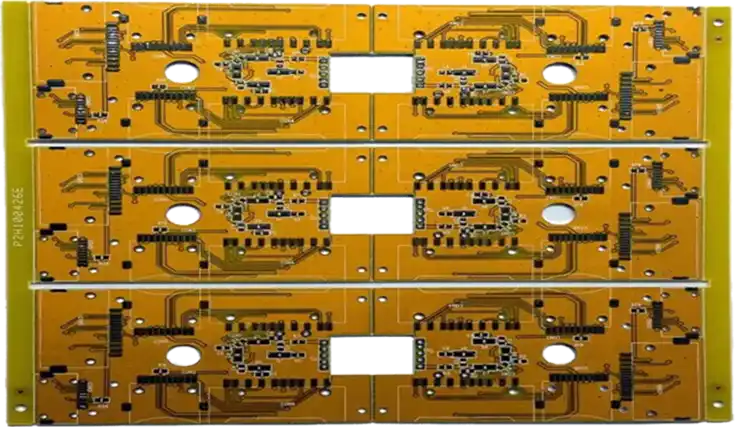
Fabrication also needs the panel construction, since the panel determines how the boards are handled through drilling, plating and routing. The tooling holes, fiducials and tab positions are part of the same package, and they interact with the board outline. The constraints involved are described in this discussion of board outline and mounting design.
<img src="https://www.gopcba.com/wp-content/uploads/2024/09/Turnkey_PCB_Assembly.webp" alt="DFM feedback loop between designer and fabricator” />
Process Capability as a Design Input
`r`n
Process capability is the term that ties the two stages together. It describes what the fabrication line can hold consistently, as opposed to what it can achieve on a good day, and it is expressed as a set of minimum features with tolerances attached. A design that works within the stated capability is built at the expected yield; one that relies on the best-case figure will produce boards that pass and boards that fail with no obvious difference between them.
`r`n
Where a design deliberately exceeds the standard capability, the reason should be recorded, because the fabricator will otherwise assume the violation is an oversight and adjust it. Adjustments made without the designer’s knowledge are the most common source of a board that differs from its documentation.
`r`n
Where the Two Sides Meet
The interaction becomes concrete at four points. The first is the minimum feature size: the narrowest trace, the smallest gap, the smallest hole and the tightest registration the process can hold. A design that stays inside those limits is built without discussion; one that exceeds them is either rejected or built at a lower yield.
The second is the aspect ratio of the plated holes. A hole whose depth is large relative to its diameter cannot be plated reliably, and the drilling and plating capability of the supplier sets the limit. Aspect ratio is a hard constraint that cannot be negotiated away by widening a tolerance.
The third is the surface finish, which affects both solderability and the cost of the board. The fourth is the laminate, whose glass transition temperature must be adequate for the assembly process, particularly where lead-free soldering is used. The differences between alloy families and their process temperatures are described in this article on lead-free and leaded solder.
DFM Feedback
The design for manufacture review is where the loop closes. The fabricator examines the artwork, identifies features that are difficult or impossible to produce, and either adjusts them or reports them. Line widths may be compensated for the etch factor, pads may be trimmed to satisfy a clearance rule, and clearances may be widened where the process requires it.
Those adjustments are normal, but they change the board that is built relative to the data submitted. A designer who is told that a pad was trimmed learns something about the clearance rules that caused it and can avoid the same violation in the next design. A designer who is not told learns nothing, and the same adjustment is repeated indefinitely.
Good practice is therefore to request a report of the changes made, and to treat the adjusted artwork as the design of record for that revision. The techniques the fabricator applies are described in this discussion of HDI board CAM methods.
Making the Loop Work
A design handoff is the moment when the layout becomes someone else’s responsibility, and its quality determines how smooth the transition is. A handoff that includes the stack, the impedance targets, the finish, the panel construction and the acceptance criteria leaves nothing to be inferred, while one that delivers artwork alone invites the fabricator to make assumptions. A short loop is a competitive advantage. The measures that shorten it are unremarkable: publish a design rule set that matches the chosen fabricator”s capability, verify the component library once rather than per project, agree the stackup early, and include the fabrication data with the layout rather than after it. Each of those removes a round of questions, and each round that is removed is schedule recovered.
The physical requirements that a board must satisfy before it leaves fabrication are described in this discussion of multilayer prototype requirements, and they form the natural acceptance criteria for the first pass through the loop, which is the point at which the design either confirms its assumptions or returns for another cycle.
FAQ
When should the fabricator be involved in a design? Before the stackup is fixed. The stack determines the impedance calculations, the trace widths and the assembly process, and a stack chosen without knowing what the fabricator can build usually has to be changed after routing, which invalidates the layout.
Why does the fabricator change my artwork? To make it producible: line widths are compensated for the etch factor, pads are trimmed to satisfy clearance rules, and dimensions are adjusted to the process window. The changes should be reported so the designer understands what the delivered board actually contains.
What information must accompany a layout to fabrication? The layer stack with materials and thicknesses, the finished thickness and tolerance, the copper weight per layer, the surface finish, the mask and silkscreen requirements, the impedance targets where applicable, and the acceptance criteria for inspection.