RF Board Layout: Partitioning to Reduce Signal Coupling
Radio boards are usually described as difficult, and most of the difficulty comes from signal coupling rather than from the active circuitry. A receiver that works on the bench can lose sensitivity once the transmitter beside it starts switching, not because any component is wrong but because energy found a path it should not have taken. RF board layout is largely the business of deciding where that energy is allowed to go, and partitioning is the tool that makes those decisions systematic.
Why Partitioning Comes First
Modern products integrate analog, digital and RF blocks in a very small volume. Multi-function chips put RF, intermediate frequency, analog and digital signals on the same die and bring their pins out side by side, where they are electrically unrelated but physically adjacent. Supply rails multiply as well, since different blocks are powered down independently to save battery life, and a phone may need five or six separate operating rails. In that environment, placement and partitioning decide performance before any routing rule is applied.
Partitioning means separating the board into physical and electrical regions. The physical side covers placement, orientation and shielding. The electrical side covers power distribution, RF routing, sensitive circuits and grounding. Both have to be planned at the start, because they are expensive to change once the layout is dense.
Physical Partitioning: Placement and Orientation
The most effective method is to fix the components on the RF path first and orient them so that the path is as short as possible, the input is far from the output, and high-power stages are separated from low-power stages. A high power amplifier and a low noise amplifier should be placed as far apart as the board allows. When space is tight, putting them on opposite sides of the board, or arranging them to operate at different times rather than simultaneously, is a reasonable compromise.
Linear blocks such as multi-stage amplifiers provide useful isolation simply by occupying space between RF regions. Duplexers, mixers and intermediate frequency amplifiers do not, because they carry several signals at once; these need deliberate separation and, where possible, a grounded barrier between the two paths.
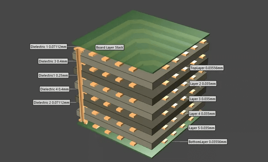
The stackup and the ground structure carry the electrical half of the partitioning, and impedance matching is what makes the physical separation electrically effective.
Electrical Partitioning: Supply and Ground
The preferred stackup places the main ground plane on the second layer, directly below the surface, and routes the RF path on the top layer. Keeping the via count on the RF path small reduces path inductance, limits leakage into the inner layers and avoids interruptions in the reference plane. Each functional block should have its own decoupled supply, with the decoupling placed at the point where the supply enters the block rather than at the far end of a shared rail.
Ground is the reference for every one of those blocks and the return path for every signal. A solid ground plane provides the best isolation between regions, because it gives return currents a continuous path beneath the signal. Splitting the plane into labeled analog, digital and RF sections seems attractive, but in practice high-speed signals cross between the sections and the split creates more problems than it solves.
Ground Plane Strategy and Stitching
The practical alternative to splitting is a single ground plane with disciplined routing above it. Fill ground copper on every layer, connect it back to the main ground plane with plenty of stitching vias, and place those vias so that they form barriers between regions where required. Vias around the edge of an RF block, spaced a small fraction of a wavelength apart, create a fence that suppresses lateral wave propagation.
Isolated copper islands should be avoided. A piece of copper that is not connected to the main ground behaves as a small antenna, picking up energy in one place and radiating it in another. If a copper region cannot be stitched to ground, removing it is usually better than leaving it floating.
With the regions defined and the reference plane in place, the remaining work is controlling the paths between them.
Controlling Coupling Between Traces
RF output must be kept away from RF input, and both must be kept away from sensitive analog and fast digital signals. Where traces must cross, crossing at right angles minimizes capacitive coupling, and running a ground trace between them along the RF line adds isolation. Where traces run in parallel, reducing the spacing increases inductive coupling, so parallel runs on sensitive nets should be kept short and separated, following the same 3W spacing discipline used on high-speed digital boards.
Ground copper should surround RF traces, pads and components wherever the geometry allows, with stitching vias tying the copper to the main ground. This provides a local shield and a controlled return path. Shielding cans over sensitive blocks are effective, but they should be planned into the placement so that the components fit under the can and the fence vias line up with its walls.
Sensitive Blocks: Oscillators, Resonators and AGC
Voltage controlled oscillators, resonator circuits and automatic gain control stages are the parts most likely to misbehave. A resonator typically contains a number of components spread over a wide area while operating at a high frequency, and it is very sensitive to noise; the components have to be placed close together and connected back to the control loop with short, direct traces. The oscillator often sits at the end of the RF region and may need its own shield.
Automatic gain control amplifiers must handle large and rapid changes in signal strength, which means a wide bandwidth and a correspondingly wide window for noise. Good analog practice applies: short input pins, a short feedback path, both kept away from RF, intermediate frequency and high-speed digital traces, with well decoupled supplies. Where a long trace is unavoidable, it belongs on the output, which is the lower impedance node.
Layer Changes and Via Placement
Every layer change is an opportunity for energy to leak from one side of the board to the other. Through vias that pass completely through the board couple the top and bottom regions, which can defeat the separation achieved by placement. Blind vias that connect only the layers involved in the transition reduce that leakage, at the cost of a more expensive fabrication process.
Where through vias are unavoidable, they should be located in areas that are not part of any RF path, and the copper around them should be stitched to ground so the transition stays controlled. Power distribution through the same region should be filtered to keep switching noise out of the RF supplies, and the overall ground and power routing plan should be drawn before signal routing begins.
FAQ
Should I split the ground plane into analog, digital and RF sections? Usually not. A solid plane with disciplined placement and stitching provides better isolation, because split planes force return currents to detour. Reserve splits for genuinely isolated interfaces.
How far apart should the power amplifier and the receiver be? As far as the board allows, and on opposite sides if necessary. Isolation improves by roughly 6 dB each time the separation doubles, so distance is the cheapest isolation available.
Are shield cans necessary on every RF block? No. They are justified on oscillators and the most sensitive receivers. Placement, ground fencing and short paths usually solve the rest, and a can adds cost and assembly steps.