Micro Assembly Technology for Small Batch SMT
Micro assembly is the practice of placing bare die and very small components onto a high-density interconnect substrate and sealing the result into a single package. It is the technology behind multi-chip modules, sensor packages and the compact radio and power modules that appear inside consumer products. Its constraints differ from those of ordinary surface mount assembly, and they affect the substrate design as much as the process.
What Micro Assembly Covers
The term covers assembly on a substrate that is itself a high-density board: fine traces, small vias and often multiple layers. Components are attached by the same general processes used for surface mount, but the scale is smaller, and the range includes bare semiconductor die that are bonded directly rather than packaged parts.
The result is a module that integrates functions which would otherwise occupy separate packages. The advantage is not only size. Integrating several devices on one substrate shortens the connections between them, which reduces parasitic inductance and improves behaviour at high frequency, and it allows the thermal path to be designed as part of the substrate rather than left to each package.
Multi-Chip Modules
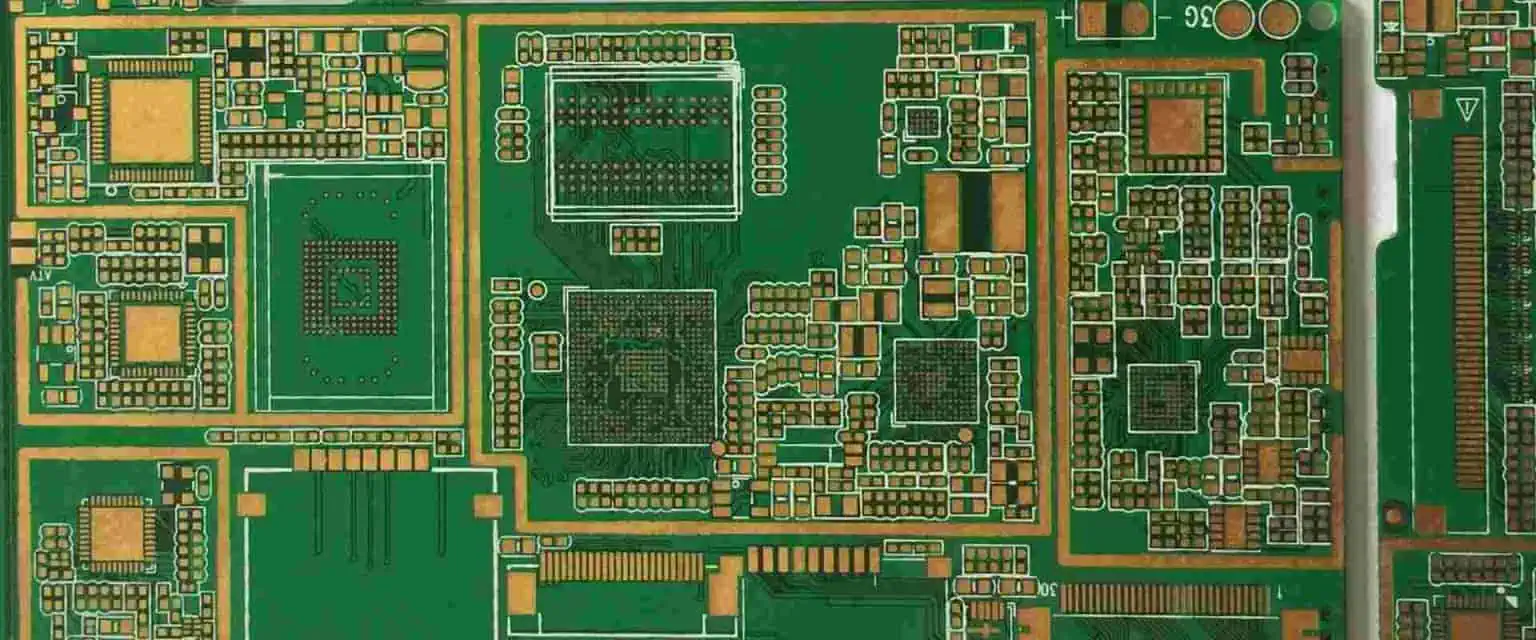
A multi-chip module places several integrated circuits on one substrate and connects them within the module before the module is sealed. The substrate may be ceramic, laminate or a combination, and its function is to provide both the interconnect and the thermal path.
The assembly steps are the attachment of each die to the substrate, the electrical connection of the die to the substrate pattern, the connection of the substrate to the package, and the sealing of the whole. Each step has its own tolerance, and they accumulate across the module. Because the dies cannot be replaced once the module is sealed, the yield of the whole assembly depends on the yield of each die and on the accuracy of each placement, which is why module assembly is normally performed in a controlled environment with in-process inspection at each stage.
Flip Chip and Wire Bonding
Two interconnection methods dominate. Wire bonding connects the die to the substrate with fine wires, one at a time, from the die pads to the substrate pads. It is flexible and well understood, and it is the usual choice where the connection count is moderate. Its limitation is electrical: the wires add inductance, and they occupy space around the die that cannot be used for routing.
Flip chip turns the die face down and connects it directly to the substrate through solder bumps. The connections are shorter, which reduces inductance and allows a much higher connection count in a smaller area, and the whole die footprint becomes available for connections rather than just the perimeter. The trade-off is that the substrate must be designed with a matching bump pattern, and the thermal path changes because the heat now leaves through the bumps and the underfill rather than through the die back. The substrate features that support this density are similar to those described in this discussion of HDI board CAM methods.
Substrate Design Considerations
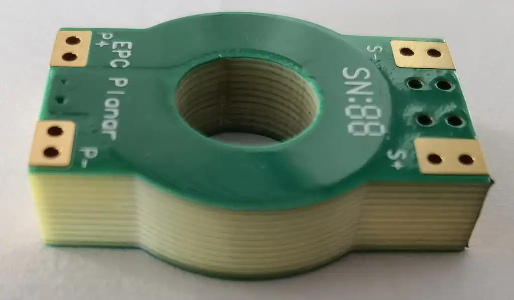
The substrate carries the same design responsibilities as any other board, at a smaller scale. The pad geometry must match the die and the component terminations exactly, because there is no room to accommodate an error. The impedance of the interconnections matters more than on a conventional board, because the traces are short and the frequencies involved are high.
Thermal design becomes part of the substrate design. A die that dissipates power must have a path through the substrate to a thermal plane or to the package base, and that path is usually built from a dense array of filled thermal vias rather than from a single large hole. The structures used to fill vias so that they can carry heat and current are described in this article on electroplating via filling.
Small Batch Considerations
Micro assembly in small volumes is a different economic problem from the same work in production. The tooling, the stencils and the placement programmes are the same cost regardless of quantity, so the per-unit cost falls steeply with volume. In small batches the design should therefore be adapted to the processes that are available rather than optimised for a process that would only pay off at scale.
That often means preferring components that can be placed with standard equipment, keeping the substrate within the capability of a conventional fabrication process, and accepting a slightly larger module in exchange for a process that works on the first attempt. Where a design does require a high-density substrate, the features that make it buildable are described in this discussion of via in pad and plated through holes.
Inspection and Yield
Inspection at these dimensions cannot rely on the human eye. Automated optical inspection handles the surface features, X-ray inspection reveals the connections that are hidden under a die or a package, and electrical test at the substrate level identifies opens and shorts before the expensive die are attached. Testing the substrate first is the single most effective yield measure in micro assembly, because it prevents good die from being committed to a defective substrate.
The same principle applies to the process as a whole: the earlier a defect can be detected, the cheaper it is to correct. The economics and the methods involved are described in this article on PCB electrical test coverage.
Process Control in Low Volume Micro Assembly
Low volume micro assembly lives or dies on process control rather than throughput. With small batches, the operator cannot average out variation across a long run, so each placement, each bond and each dispense step has to be right the first time. Die attach epoxy volumes measured in picolitres, wire bond loop heights of a few tens of microns and solder paste deposits on fine pitch pads all sit close to the edge of the process window, and the machine settings that produce good results on one substrate lot may need revisiting on the next.
Inspection strategy has to compensate. Visual inspection under a microscope remains the workhorse for wire bonds and die attach fillets, supported by shear and pull testing on a sample basis to confirm that the process, not just the individual unit, is under control. X-ray is used where hidden joints cannot be reached optically, and electrical test at the module level confirms the internal connections before encapsulation makes them permanent. Documenting the settings and the conditions for every batch is what turns a fragile result into a repeatable one, which is what a customer buying a small quantity of a critical module is actually paying for.
FAQ
What is the difference between a multi-chip module and a conventional assembly? A module places several die on one substrate and connects them within it before sealing, so the module behaves as a single component. That shortens the interconnections between the devices, reduces parasitic inductance and allows the thermal path to be designed as part of the substrate.
When is flip chip preferred over wire bonding? When the connection count is high or the electrical performance matters. Flip chip connections are shorter and can be much more numerous in the same area, at the cost of a substrate that must be designed with a matching bump pattern and a different thermal path.
Why test the substrate before attaching the die? Because the die are the most expensive parts of the assembly and cannot be recovered if the substrate is defective. Testing the substrate first prevents good die from being committed to a board that will fail, which is the largest single yield improvement available in micro assembly.