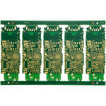
Power Plane Inset in Multilayer Boards: Why and How Much
On a multilayer board the power and ground planes are usually the largest copper features in the design, and where they stop matters. A plane that runs all the way to the board edge presents an exposed copper edge to the outside world, and no amount of decoupling will fix the radiation that results. Insetting the plane is a cheap control, provided the amount is chosen deliberately rather than copied from a template.
What the Inset Is and Why It Exists
A power plane inset is the distance the plane is pulled back from the physical board outline. The rule of thumb that circulates most widely is 20H, where H is the dielectric thickness between the plane and the reference plane next to it. The purpose is to keep the fringing field that exists at the plane edge well inside the board outline, so that the edge of the laminate does not become an efficient radiator.
The Physics in Plain Terms
A power and ground plane pair behaves like a parallel-plate transmission structure with an open edge. At the edge, the field is not confined and the structure radiates, much as a slot antenna does. The larger the exposed edge relative to the wavelength, the more efficient that radiation becomes, which is why the effect is worst on large planes and at high frequencies.
Pulling the plane back moves the radiating edge away from the laminate edge. The field still fringes beyond the copper, but the fringing decays with distance, and once the plane edge is far enough inside, the field reaching the board edge is small.
How 20H Works Out in Numbers
The thickness H is the dielectric between the plane pair, not the whole board. On a four-layer board with a 0.2 mm core between the power and ground layers, 20H is 4 mm, which is usually more copper than the design can give up. In practice most boards use between 5H and 10H and accept a slightly higher edge field.

The useful way to apply the rule is to scale it: 0.5 mm is a reasonable minimum inset on a standard four-layer board with a thin dielectric, and 1 to 2 mm is appropriate for a thick dielectric or a large high-speed board. Where the plane pair is close together, 20H is small and achievable, which is one of the incidental benefits of a thin dielectric between power and ground.
What the Inset Costs
Every millimetre of inset is copper removed from the plane, which raises the plane impedance and reduces the distributed capacitance between the planes. On a design that already has marginal decoupling, a large inset makes the power distribution network worse at the same time as it improves the radiated field.
The compromise is to keep the inset modest on the power plane and larger on the ground plane, since the ground plane is the reference for most of the routing and its edge is the more significant radiator. Where a plane must reach the edge for a functional reason, the acceptable answer is usually to accept the radiation and deal with it by other means.
Inset at Edges That Are Machined
Scored and routed edges need different treatment. A V-cut scores the laminate from both sides, and the score line cuts into the material between the planes, so a plane that approaches a scored edge can be exposed after depanelling and can even short to the scoring blade. Planes should be pulled back from any scored edge by at least the depth of the score plus a margin.
<img src="https://www.gopcba.com/wp-content/uploads/2026/08/flexible-pcb-assembly-cover.jpg-1.webp" alt="plane pullback at a scored edge on a multilayer PCB” />
Castellated holes and edge plating create a deliberate connection to the board edge, so the plane inset rule does not apply in the same way. What applies instead is that the plane has to be connected to those features by design and not by accident. PCB slot design rules and edge routing covers the edge features that interact with plane geometry.
Inset Versus Plane Splitting
Inset is an edge treatment and splitting is an interior treatment, and they solve different problems. Splitting a plane creates islands for different voltages, and each split introduces a discontinuity in the reference that signals must not cross. Insetting keeps the plane continuous but shrinks it. A design with several rails needs both: islands inside the board, and a controlled pullback at the perimeter.
The two interact where a split approaches the edge. The island that results can be small enough that its own inset is meaningless, and the routing over it has no reference at all. Power plane splitting rules explains how to keep the islands functional.
Creepage and Clearance Override EMC
On any board that carries mains or another high voltage, the plane inset is set by safety requirements rather than by radiated emissions. The required creepage and clearance distances, taken from the applicable standard for the working voltage and the pollution degree, are usually much larger than 20H, and they apply to the copper at the edge including the planes.
Where both requirements apply, the larger one governs. The plane does not need to be inset further than the safety distance, but it must never be inset less.
Practical Guidance
Start from the dielectric thickness between the plane pair, apply the 20H rule as a target, and then reduce the inset until it either meets the copper area the power distribution network needs or reaches the safety distance, whichever comes first. Keep the ground plane inset at least as large as the power plane inset. Pull planes back from scored edges by more than the score depth.
Check the result in simulation if the design is sensitive. Edge radiation is difficult to predict analytically, but the trend is clear, and a board with a well-controlled perimeter is easier to pass than one without. EMI suppression design principles covers the other layout measures that work alongside the inset.
When a Plane Should Reach the Edge
There are cases where the plane extends to the edge deliberately. A board that plugs into a backplane may use the plane as a shield, and an RF board may want the ground plane to meet the enclosure wall. In those cases the radiation path is controlled by the mechanical design instead, which is a legitimate trade as long as it is made consciously.
What is not legitimate is leaving the plane at the edge because nobody changed the default. On many four-layer boards the plane polygon is drawn by copying the outline and shrinking it by a token amount, and that token amount is not a design decision. It is worth checking the perimeter geometry explicitly before the board is released, especially on designs where the enclosure is plastic and the board edge is fully exposed.
FAQ
Is 20H a hard requirement? No. It is a rule of thumb that reduces edge radiation substantially where it can be applied. Most production boards use less and control emissions by other means.
Should the ground plane be inset more than the power plane? Usually yes. The ground plane is the reference for the routing and its edge is the more significant radiator, so a slightly larger inset on the ground plane is a reasonable default.
Does the inset affect impedance? Not for the traces above the plane, provided they stay over solid copper. It does affect the plane impedance and the distributed capacitance between power and ground, which is why the power plane inset is kept modest.