SMT Micro-Assembly Technologies: MCM, Flip Chip and PoP
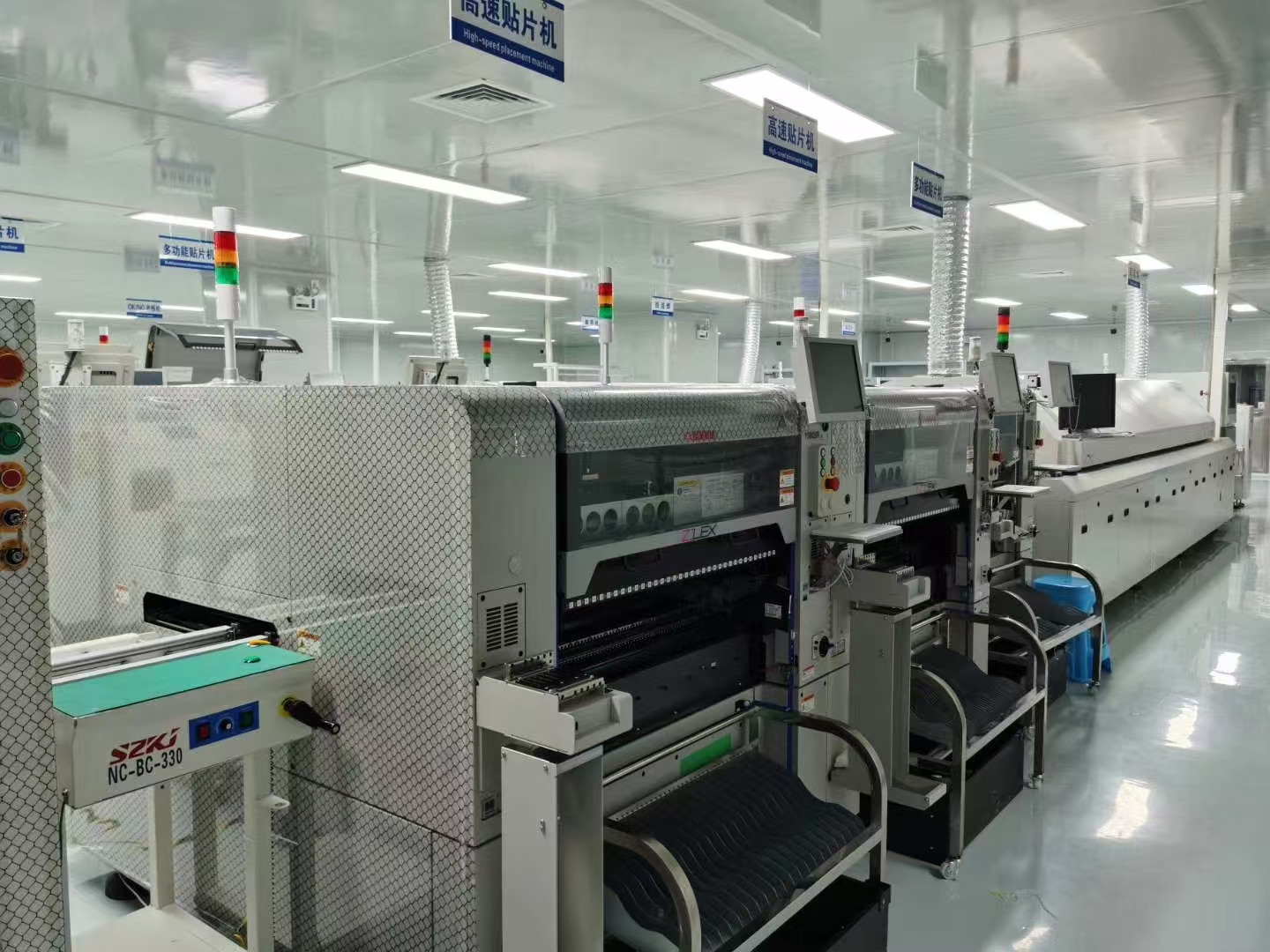
Micro-assembly is the bridge between a finished circuit board and a working miniature product. It combines fine-pitch soldering, die-level interconnection and package stacking on a high-density interconnect substrate, and it is normally applied to small and medium production batches where a full chip-scale supply chain is not justified. The four families below cover most of what appears in that work, and each one imposes its own constraints on the board underneath it.
What micro-assembly covers
The goal is to assemble miniature components on a dense multilayer interconnect substrate using soldering, bonding and encapsulation to form a functional microelectronic assembly. That definition stretches from an ordinary fine-pitch surface-mount build to a module containing bare dies and optical waveguides. What these techniques share is that the substrate is no longer just a carrier: its routing density, its thermal path and its surface finish all become part of the electrical design. Deciding which micro-assembly technologies apply should happen while the substrate is still being laid out, because most of the constraints are fixed by then. The same is true of the thermal path: a module that dissipates several watts through a small footprint needs copper area, thermal vias and a defined attachment surface on the substrate, and no amount of process control at the assembly stage can compensate for a board that was never designed to carry that heat away.
Multi-chip module assembly
A multi-chip module takes several large-scale integrated dies and mounts them at high density on a multilayer interconnect substrate, which is then sealed into a single package. The approach grew out of hybrid integrated circuits and delivers a compact assembly that behaves electrically like one component. The assembly sequence covers three connections: attaching the die to the substrate mechanically, connecting the die electrically to the substrate, and connecting the substrate to the package both physically and electrically. Because the dies sit close together, interconnect length between them is short, which is the main electrical benefit and the reason the technique appears in high-speed and mixed-signal designs. The penalty is thermal density: heat is generated in a small area and must be conducted through the substrate.
Flip chip interconnection
Conventional wire bonding places connections around the perimeter of the die, so the number of inputs and outputs is limited by the die edge. Flip chip reverses the die face down and connects through bumps distributed across the whole die surface, which raises the available connection count substantially and shortens the interconnect path. Because the entire area is usable, the package can be smaller for the same function, and the inductance of the connection drops. The practical variants include solder-paste flip chip assembly, stud-bump bonding, and the controlled-collapse chip connection known as C4, in which the solder bump itself defines the standoff and self-aligns during reflow. Each variant changes the substrate finish, the bump pitch and the underfill requirement, so the choice has to be made with the fabricator, not after the substrate is ordered.
Package-on-package stacking
Package-on-package assembly stacks a memory package on top of a logic package, and in doing so it blurs the line between first-level packaging and second-level assembly. The bottom package carries the high-density digital or mixed-signal logic, while the top package carries high-density or combined memory devices. Stacking raises the logic and memory capacity available in a given footprint and lets the customer choose the memory configuration at assembly time rather than at wafer level, which also controls cost by allowing one logic package to serve several product variants. For the substrate designer, the consequence is a tighter requirement on the package footprint, the ball pitch and the routing that must escape from beneath the lower package.
Optoelectronic interconnect
Optoelectronic board-level packaging integrates optical devices with electronic packaging on the same substrate, producing an assembly that carries both electrical and optical signals. That assembly behaves as a special multi-chip module containing an optical circuit substrate, optoelectronic devices, optical waveguides, fibers and optical connectors. The interesting property is that copper conductors carrying electrical signals and optical paths carrying light can be fabricated on one substrate, so a board can move high-bandwidth data optically while keeping conventional power and control routing in copper. Optical assembly is usually described as a hierarchy of six levels: chip, device, module, board, subsystem and system. Each level has its own alignment tolerance, and alignment error accumulates upward, which is why optical assemblies specify tighter mechanical tolerances than purely electrical boards.
What this means for the substrate design
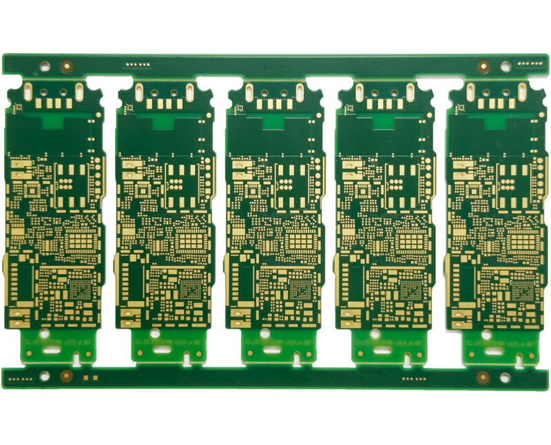
Every one of these techniques pushes requirements back onto the board. Flip chip demands a very flat surface and a defined bump pattern with a solder mask that will not interfere with the bump land. Multi-chip modules and optical assemblies demand controlled impedance and low-loss dielectric, which is why high-speed multilayer construction is usually the starting point. Package-on-package demands a dense escape pattern under the lower package, which is exactly the problem that multilayer boards solve for high-speed designs. Optical integration adds alignment features and mechanical datums that must be held across the whole panel.
Micro-assembly also changes the volume economics. The tooling and engineering effort are worthwhile when the product is small or medium volume and the substrate carries a lot of functional value, which is common in medical, instrumentation, aerospace and communications equipment. Working through the PCBA development process at the start, and confirming that the substrate can support the required bump pitch and via structure, avoids the situation where the assembly plan is sound but the board cannot be built. Where the micro-assembly sits next to high-speed interfaces, the guidance collected for high-speed interfaces on FPGA boards applies directly to the escape routing. gopcb reviews the substrate and the assembly route together so that the two plans match.
Die attach, underfill and encapsulation
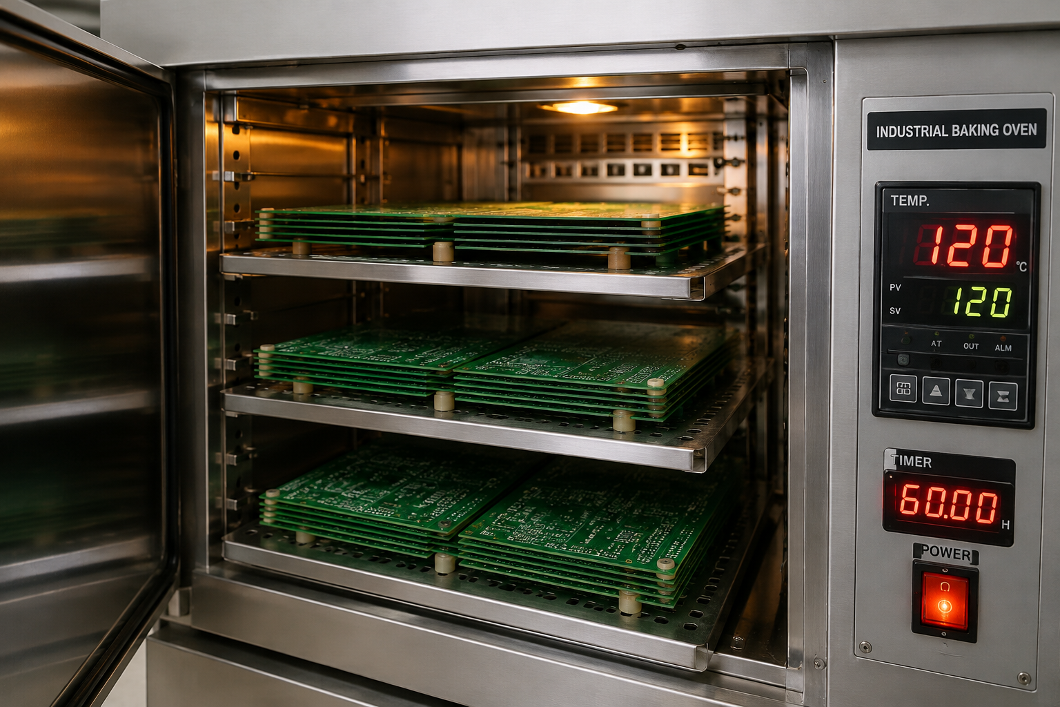
The electrical connection is only part of a micro-assembly. A die must first be attached to the substrate with a material that holds it in place, conducts heat away and does not introduce stress as it cures. Adhesive selection therefore trades thermal conductivity against cure temperature and modulus, and a mismatch in thermal expansion between the die and the substrate is what drives the choice toward a compliant material. Once the interconnect is formed, underfill flows into the gap beneath a flip chip and mechanically couples the die to the substrate, spreading the stress that would otherwise concentrate in the bumps during thermal cycling. The final encapsulation step protects the assembly from moisture and handling damage. Each of these materials has a cure schedule, and the schedule has to be compatible with the substrate and with any components already soldered onto the board.
FAQ
Is micro-assembly only for very large volumes? No. It is most often applied to small and medium batches where the product carries high value and the circuit density is high. The tooling cost is the deciding factor, not the batch size alone.
What is the main advantage of flip chip over wire bonding? Flip chip uses the entire die surface for connections instead of the perimeter, so it supports far more inputs and outputs and shortens the interconnect path. It also removes the loop inductance that a wire bond introduces.
Why does optoelectronic assembly need tighter tolerances? Optical coupling depends on physical alignment between the device, the waveguide and the fiber. Alignment error accumulates through the six levels of the assembly hierarchy, so each level has to be held tighter than a purely electrical board would require.