EMC Design for Switching Power Supply PCB Layout
Switching supplies are among the most demanding boards to lay out for electromagnetic compatibility, because the interference is generated by the circuit’s normal operation rather than by a fault. Currents and voltages change rapidly by design, the switching node is a small antenna, and the control circuitry that must remain undisturbed sits centimetres away from the source. Adding a filter at the end is expensive and often insufficient, so the layout itself has to do most of the work. Good EMC design for a switching supply is therefore mostly a matter of controlling where the fast currents flow and how large the loops that carry them become, and those decisions are made long before any filter value is chosen. A layout that ignores them can usually be made to pass with enough filtering, but the cost and the volume of that filtering are paid on every unit.
Why Switch-Mode Supplies Behave Differently
A digital board and a switching supply both contain fast edges, but the supply has a much clearer separation between aggressor and victim. The sources are concentrated in a few components: the power switch, the fast recovery diode, the transformer or inductor, and the wires connecting them. The victims are equally identifiable: the control circuit, the feedback network and any line that runs to a measuring instrument. That separation is an advantage, because it means the interference can be attacked at a small number of well-defined places rather than everywhere at once.
Conducted Interference and Shared Impedance
Conducted interference reaches a victim through the conductors that connect the two. In a supply this happens in two ways. The first is direct coupling through the wiring, where a fast switching current flows through a common conductor and the voltage it develops appears at another circuit. The second is common-impedance coupling, where two circuits share a conductor and the current of one produces a voltage across that shared impedance which is then seen by the other. The practical consequence is that the ground return is never a perfect reference, and the layout must minimise the length of conductor that two circuits share. Separating the power return from the control return, and bringing them together only at the point where the supply output is measured, removes most of this mechanism. The layout practices that control the return path are described in this article on radiated EMI in switching regulator layout.
<img src="https://www.gopcba.com/wp-content/uploads/2026/08/iStock-1307839840-jpg-1.webp" alt="switching power supply PCB with input filtering and ground plane” />
Crosstalk Between Traces and Cables
Crosstalk is one of the hardest problems to eliminate once a board is built, because it depends on geometry that is fixed. It is expressed through the mutual capacitance and mutual inductance between two conductors: an electric field couples through capacitance and a magnetic field through inductance, and which one dominates depends on the impedance of the circuit and the frequency. Where a control or logic line runs parallel to a low-level signal line, interference is likely once the parallel run exceeds about 10 cm, and long cables carrying several high-speed data lines alongside control wiring behave the same way. In general, capacitive coupling dominates at high frequency, while inductive coupling dominates at low frequency and low circuit impedance. Where a cable is shielded and the shield is grounded at both ends, the magnetic coupling becomes the dominant path instead. The same spacing discipline that applies to signal traces applies here, and the simplest formulation is given in the 3W rule for crosstalk.
Radiated Emissions
Radiated interference is coupled through the air rather than through a conductor, and it falls into two categories. Differential-mode radiation comes from the loop formed by a signal and its return, and it is proportional to the area of that loop and to the rate of change of the current in it. Common-mode radiation comes from the whole cable or structure acting as an antenna, driven by a voltage that appears between the circuit ground and the chassis. In a switching supply the common-mode component is usually the larger contributor, and its radiated effect is generally far greater than that of the differential component, so reducing common mode is where most of the benefit lies. That means controlling the parasitic capacitance between the switching node and the chassis, keeping the transformer’s inter-winding capacitance in mind, and providing a low-impedance path for the common-mode current to return to its source.
Layout Measures That Do Most of the Work
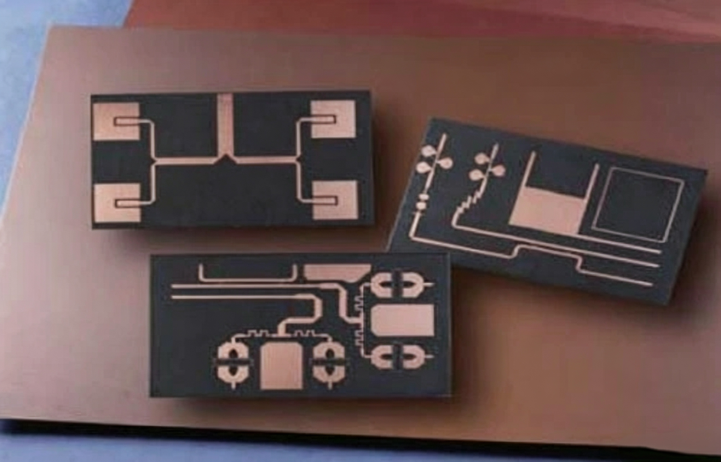
The highest-value measures are geometric. The switching loop, made up of the input capacitor, the switch and the return path, should have the smallest possible area, because that loop is the source of both differential radiation and much of the conducted noise. The ground plane under the power stage should be unbroken, and the control circuitry should reference the same plane rather than a separate island. Wide copper for the return paths lowers the impedance that a disturbance has to develop voltage across. Sensitive nodes such as the feedback divider and the current-sense input should be kept short, away from the switch node and away from the inductor, and their return should be taken from a quiet point. Where a plane must carry both the power return and the control return, the two should be joined in a way that does not force the control current through the power path. The trade-offs between a solid plane and a meshed copper area are covered in this article on copper flooding, mesh or solid.
Filtering and Damping
Filtering is used to keep the remaining interference from leaving the board, and its position matters as much as its values. An input filter should be placed at the point where the supply connects to the outside world, with its return taken directly to the same ground the power stage uses, so that the filter is not bypassed by a current path that runs around it. Snubbers across the switch or the diode reduce the ringing at the source, but their components must be mounted with the shortest possible leads, because the inductance of the connection can cancel the benefit at the frequency that matters. The same principle applies to capacitors on the switching node, where lead length has more influence on effectiveness than nominal value.
Verifying the Result
Because the mechanisms are predictable, they can be measured rather than guessed. Conducted emissions measured on the input leads and radiated emissions measured in a chamber show which mechanism dominates, and near-field probing of the board shows where the strongest fields are concentrated. Where a limit is exceeded, the measurement usually identifies whether the problem is a loop, a shared impedance or a common-mode path, and the fix should be applied at that point rather than by adding a general-purpose filter. The principles behind those measurements are described in this article on EMI suppression design principles.
FAQ
Which coupling mechanism dominates in a switching supply? Common-mode coupling, in most cases, because the whole cable or enclosure acts as an antenna driven by a voltage between the circuit ground and the chassis.
Is capacitive or inductive crosstalk more important? Capacitive coupling usually dominates at high frequency, while inductive coupling dominates at low frequency and with low-impedance circuits.
How long can two traces run in parallel before crosstalk becomes a concern? Around 10 cm is the practical threshold for control and low-level signal lines, after which the coupling should be evaluated rather than assumed acceptable.