



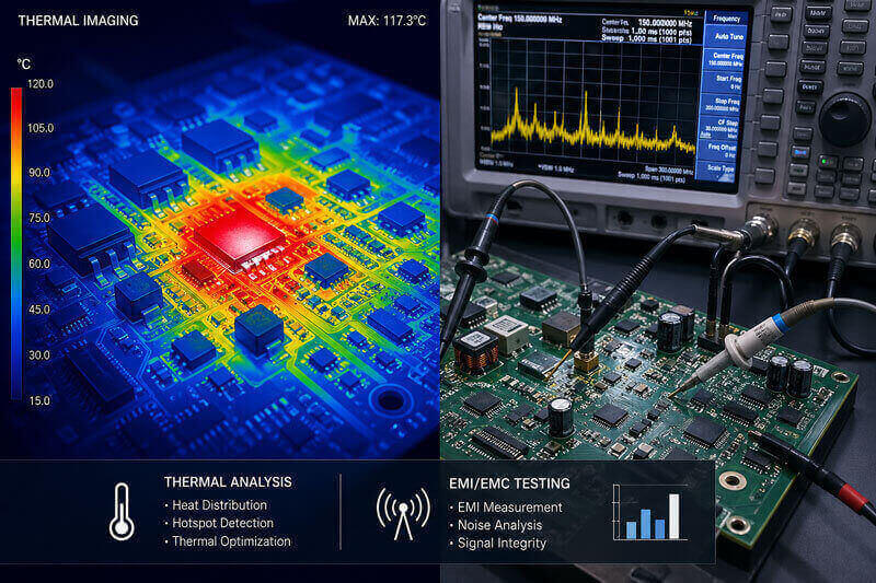
Radiated EMI in Automotive Power Supply Layout
Board layout decides the fate of every power supply. It determines whether the circuit functions, how much electromagnetic interference it emits, and how hot it runs — and it does all three at once. Switching regulator layout is not a mystery and it is not difficult, but it is often deferred during the early design phase. Since the requirements for functional stability and for low emission usually point the same way, there is no reason to wait: a good layout designed in from the start costs nothing extra, and it saves money by removing the need for filters, mechanical shielding, additional EMI testing and board revisions.
Conducted and Radiated Interference
Interference leaves a circuit by two routes, and they behave differently enough that they have to be handled separately.
Conducted EMI travels along the wires and conductors connected to the product. Because the noise is confined to defined terminals and connectors, a good layout combined with filter design will usually bring a design into compliance early in development, when changes are still cheap.
Radiated EMI is another matter. Every part of a board that carries current radiates a field; every conductor on the board is an antenna, and every copper plane is a resonator. Any signal that is not a pure sine wave or a DC level generates noise across the whole signal spectrum. Even a carefully designed board will not reveal how severe its radiated emissions are until the system is tested, and formal radiated testing cannot realistically be performed until the design is essentially finished — which is precisely why the design has to be right beforehand.
Filtering attenuates interference at a specific frequency or across a band. The portion that travels through space can be reduced with metal and magnetic shielding; the portion travelling along conductors can be controlled with ferrite beads and other filters. Interference cannot be eliminated — the objective is to attenuate it to a level the surrounding digital and communication circuits can tolerate, and the limits that apply are set by regulation rather than by preference.
Why Automotive Systems Are Harder
Vehicle electronics pack a great deal of electronics into a small volume, and they do it in the presence of audio systems, radio frequency equipment, CAN buses and radar sensors. That environment magnifies a problem that exists in any design: paralleling several switching regulators to share current and deliver more output power.
When multiple regulators switch at similar frequencies, the energy each produces accumulates at the same frequency instead of being spread across the spectrum. The result is a concentrated emission that is far more consequential than the individual contributions would suggest — particularly when the board, and the boards around it, carry devices that are sensitive to energy at that frequency.
<img src="https://www.gopcba.com/wp-content/uploads/2026/08/Common_High_Frequency_PCB_Design_Mistakes.jpg.webp" alt="radiated EMI hot loop in a switching regulator layout” />
Switching Frequency Sets the Difficulty
Modern surface mount input filter components perform better than their through-hole equivalents, but that improvement has been offset by rising switching frequencies.
Faster switching transitions improve efficiency and shorten the minimum on and off times, and in doing so they generate higher harmonic content. Two rules of thumb describe the penalty. Holding everything else constant, doubling the switching frequency makes interference 6 dB worse. Broadband emission behaves like a first-order high-pass response, so raising the switching frequency tenfold adds about 20 dB to the radiated level.
It follows that the switching frequency is a design parameter with an emissions consequence, not just an efficiency and size consequence. Where the application allows a choice, the frequency band matters as much as the frequency itself — operating below or above the band used by amplitude modulated broadcast, for example, is a deliberate way of moving emissions away from a receiver that matters.
The Hot Loop
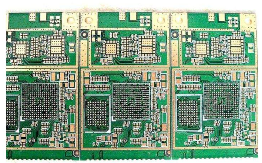
An experienced designer keeps the hot loop — the path carrying the high di/dt current — as small as possible, and places the shielding or ground layer as close as possible to the active layer.
The achievable minimum is not unlimited. It is constrained by the device pinout, the package construction, the thermal requirements of the design and the package size needed to store sufficient energy in the decoupling capacitors. These pull in different directions, which is why the smallest loop is a design outcome rather than a layout preference.
There is a second, less obvious limit. In a typical planar board, magnetic or transformer-type coupling between conductors above roughly thirty megahertz defeats the effort put into filtering, because unwanted magnetic coupling becomes more effective at higher harmonic frequencies. In practice that means the higher harmonics escape through coupling between traces rather than through the filter, which is described from the mechanisms side in this overview of EMI sources and coupling paths.
The Available Remedies
Because interference cannot be removed, the options are about where to spend.
A shielded enclosure is the most thorough approach: putting the whole circuit inside a shield box removes the problem rather than attenuating it. The costs are real and predictable — higher material and assembly cost, more board space consumed, and a much harder thermal and test situation, since the box that keeps fields out also keeps heat in and blocks access.
Slowing the switching edges reduces emissions without adding a shield, but it degrades efficiency, lengthens the minimum on and off times, introduces associated dead time and limits how fast the current control loop can respond. It is a genuine trade rather than a free improvement.
Layout-based reduction is the cheapest and the most frequently skipped. Minimising the hot loop, placing the input capacitor so that its loop is as tight as the pinout allows, returning the switching current directly beneath the components that carry it, and keeping the switch node copper no larger than necessary all reduce the radiating area. Avoiding long stubs and isolated copper that act as antennas is part of the same effort, and the geometry of a switching stage is examined in detail in this note on half-bridge converter layout.
Filtering then handles what remains, applied with the knowledge that a filter which reduces emissions at one frequency can be bypassed by coupling at another. Where the design has to be compliant on the first attempt, the layout should be treated as the primary control and the filter as the secondary one, an approach that follows the same logic as EMC design from the layout stage.
Design It In Early
Three decisions account for most of the outcome.
Place the input capacitor as close as the device pinout permits, and connect it with the shortest possible return path to the same ground reference as the device. This single arrangement reduces both the loop area and the impedance that produces the high frequency content in the first place.
Keep the switch node copper small. It is the noisiest node in the circuit and it radiates in proportion to its area, so making it generous in the interest of current carrying is a mistake — the current-carrying requirement belongs to the inductor and the power path, not to the node itself.
Provide a continuous ground beneath the power stage. A ground plane under the components gives the returning current a defined and short path, and reduces the loop area without any change to the schematic.
FAQ
Can good layout really remove the need for a shield? It can bring a design into compliance without one in many cases, because it reduces the radiating loop area at the source. Whether it is enough depends on the switching frequency, the power level and the limits that apply.
Why is radiated EMI harder to design for than conducted EMI? Because conduction is confined to known conductors and can be filtered at a defined point, whereas radiation depends on every current-carrying feature of the board and can only be confirmed by testing a nearly complete design.
Does running several regulators together really make emissions worse? Yes, when they switch at similar frequencies. Their energy accumulates at the same frequency rather than spreading, producing a concentration that is more damaging to nearby sensitive circuits than the individual emissions would be.

1 Comment
Escape Routing Rules: Trace Width, Angles and Pad Fanout - Kingda
[…] The best escape routing also considers the reference plane. A trace that runs over a continuous plane at a controlled height has a predictable impedance, and that predictability is only maintained if the geometry stays consistent along the route. Widening a trace abruptly, or routing diagonally over a plane edge, breaks the assumption, and the penalty shows up as the kind of radiated noise described in this article on radiated EMI in switching regulator layout. […]