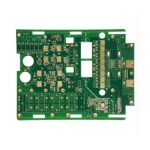
PCB Layout Basics: Footprints, Netlists, Ratlines, and Copper Pour
Most layout questions that stop a project are not about signal integrity. They are about the design database: which footprint belongs to which part, what a ratline actually means, why a netlist can differ from the schematic, and when copper pour should be added. These questions look elementary, but getting them wrong produces boards that are electrically correct and mechanically wrong, or that pass the connectivity check and fail at assembly. This article answers the ones that come up most often in PCB layout work.
The common thread is that each concept has a precise definition, and the confusion comes from using the terms loosely. Starting with the definitions makes the tools behave predictably.
Footprint and Component Correspondence
A footprint is the physical land pattern for a component: the pads, their dimensions, the spacing between them, the silkscreen outline, and the courtyard. It is a property of the package, not of the electrical function, which is why two electrically different parts can share one footprint and why the same part can exist in several.
A resistor illustrates the second case: the same electrical function may be available in multiple package sizes, and each requires its own land pattern. For that reason, when a component is placed on the board, both its name and its package must be identified. A mismatch between the package specified in the schematic and the one in the layout produces a board that cannot be assembled, and the error is not visible in a connectivity check.

Package information can be assigned in either of two places: when the schematic is drawn, by setting the footprint attribute on the component, or when the netlist is imported into the layout tool. Assigning it in the schematic is preferable, because the footprint is then part of the design data and travels with the netlist rather than being re-entered later.
Trace, Ratline, and Net
These three terms describe different things and are frequently used interchangeably. A trace, or conductor, is the copper that connects pads, and it is the physical implementation of the connection. A ratline is the thin line that the tool draws between pads that should be connected but are not yet routed; it is a graphical representation of intent and carries no electrical meaning.
A net is the logical group that includes both the traces and every pad connected to them. When a design is described as having a shorted net, the fault involves the logical group, not only the copper path. Understanding the distinction matters when reading a design rule violation: a ratline that remains is an incomplete route, while a trace that reaches the wrong pad is a connectivity error.
<img src="https://www.gopcba.com/wp-content/uploads/2021/03/h4_crs_overlay.png" alt="Net class rules and copper pour applied to a PCB layout” />
The ratline count is the practical measure of routing completeness, and it should be zero at the end of the layout, but the count alone does not prove the connections are correct. The netlist comparison against the schematic is the check that does.
Inner Layers and Mid Layers
The two terms are often confused. A mid layer is a routing layer used for conductors, and it behaves like any other signal layer. An inner layer in the traditional sense is a plane, usually power or ground, made of a continuous sheet of copper with no routing on it.
Modern CAD tools allow either, and a plane can be split into regions to carry more than one supply, with the understanding that a split plane interrupts the return path for any signal referenced to it. The distinction also affects how a layer is described in the fabrication documentation, since a plane and a signal layer are handled differently in data preparation.
Netlists and Net Classes
Two kinds of netlist exist in a design flow. The external netlist is generated by the schematic capture tool and describes the intended connections. The internal netlist is what the layout tool maintains and uses for routing; it starts from the external netlist and may be modified as the design progresses. When a design contains an unintended connection, the comparison between these two is what reveals it.
A net class is a named group of nets that share routing constraints. Grouping is useful for two reasons. First, it applies rules consistently: a class containing all the sensitive data lines can be given a larger clearance in one operation rather than net by net, and a class containing supply and ground nets can be assigned a wider trace width. Second, it makes the design manageable, because a large board with thousands of nets can be navigated by class rather than by individual net name.
Classes must be defined before routing begins to be useful. Adding a class after the routing is complete means re-checking every trace in the group against the new rule, which is exactly the work the class was meant to avoid.
Copper Pour and Its Ordering
A copper pour fills unused areas of a layer with copper, usually connected to the ground reference. It has two purposes: it provides additional return path and shielding, and it balances the copper distribution so that plating and etching behave consistently across the panel.
The ordering rule is that the pour is performed after routing, after teardrops are added, and after any trace adjustments. Adding a pour before the routing is complete means the pour has to be regenerated and re-verified afterwards. Where a pour is added to a layer that carries sensitive traces, the effect on trace impedance should also be checked, because copper placed close to a trace changes its impedance even when it is not connected to the signal.
Adding Test Points and Modifying Connectivity
Test pads and other non-component features need to be electrically assigned before they are useful. A pad placed on the board without a net is a mechanical feature, not an electrical one; assigning it to the appropriate net is what makes it a test point that the test program can use.
Where the connectivity of a design must be changed without altering the schematic, that change should be documented, because it creates a permanent difference between the two representations of the design. In production that difference becomes a defect the next engineer cannot explain.
Practice That Prevents Most of These Problems
Four habits remove most of the errors described above. Assign footprints in the schematic and verify them before the layout begins. Compare the netlist after every significant change rather than only at the end. Define net classes before routing. And treat the pour as the final operation, checking the result for isolated regions afterwards, as described in copper island and dead copper handling.
For a broader view of how these steps fit together, see the PCB design workflow. Assembly consequences of footprint and placement mistakes are covered in SMT component shift causes.
FAQ
What happens if the footprint in the layout does not match the package in the BOM? The assembly cannot place the part correctly. The placement program looks for a package that does not exist, or the part lands on a land pattern with the wrong pad spacing, producing an open or a bridge. The mismatch is invisible in the schematic and in the connectivity check.
Is a ratline the same as a wire? No. A ratline only indicates that two pads belong to the same net and have not yet been connected by copper. It has no electrical meaning and disappears as the routing is completed, whereas a trace is real copper and carries the signal.
When should copper pour be added to the design? After all routing, teardrops, and trace adjustments are complete. Pouring earlier means the copper must be regenerated whenever anything changes, and any stitching vias placed manually have to be re-checked after each regeneration.