Copper Island Keep or Remove: Dead Copper and the Antenna Effect
Almost every layout ends up with copper that is connected to nothing: a patch left behind after a plane is cleared, a sliver cut off by a keep-out, or a remnant of a pour that no net reaches. Manufacturers call it dead copper; designers argue about whether to delete it. The disagreement is usually caused by treating all isolated copper as one category, when the behaviour depends entirely on whether the patch is connected to a ground reference and how large it is. Deciding what to do with a copper island is therefore a question with a conditional answer rather than a rule.
The electrical argument has two sides, and both are correct within their own conditions. Understanding the mechanism behind each one makes the decision straightforward.
Why an Unconnected Patch Behaves Like an Antenna
An isolated conductor surrounded by routing is capacitively and inductively coupled to everything near it. At high frequency it resonates, and when its length approaches a fraction of the wavelength of the noise present, it radiates efficiently in both directions: it can re-radiate energy picked up from a nearby trace, and it can couple that energy into other traces as received noise.
This is the mechanism behind the antenna effect. A patch that is a quarter of a wavelength long at the frequency of interest is the worst case, and because digital edges contain energy across a wide band, a patch can be resonant at some frequency regardless of the clock rate. Removing the patch removes the resonant structure entirely, which is why dead copper is normally deleted on high-speed boards.
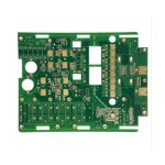
<img src="https://www.gopcba.com/wp-content/uploads/2023/05/pierre-chatel-innocenti-Lk-nu_hX6ms-unsplash.jpg" alt="PCB copper pour with isolated copper islands and stitching vias” />
The effect also depends on where the patch sits. A fragment on an inner layer, sandwiched between planes, radiates much less than the same fragment on a surface layer, because the planes shield it. That difference is why surface-layer dead copper deserves more attention than inner-layer remnants.
When Isolated Copper Helps
Keeping the copper is not irrational. Copper that is present but empty of connections still contributes mechanical stiffness, and on a large or thin board a local absence of copper creates an imbalance that can cause warpage during processing and handling. Filling the empty area also avoids the visual and process irregularity of a board with large blank regions.
More importantly, copper that is properly tied to the ground reference is not dead at all. Once it is connected to ground through multiple vias, it becomes part of the reference structure: it provides a return path, it shields adjacent traces, and it continues to support the mechanical function. The mistake is to leave the copper floating and expect it to behave as though it were grounded.
Ground Stitching and the Connection Requirement
The connecting structure is what transforms an isolated patch into a useful plane, and a single connection is not sufficient. Each connection has inductance, and the return current has to travel to that point before it can use the plane, which creates exactly the small loops the plane was supposed to eliminate.
The accepted practice is a ground stitching via pattern distributed across the copper, with spacing small enough that the plane behaves as a continuous reference at the frequencies present. A working rule for high-frequency designs is to keep via spacing below one twentieth of the wavelength at the highest significant frequency, which keeps the structure electrically short. The same spacing rule applies to copper along the board perimeter and around connectors.
Where a patch is too small to accept a via, or too far from the ground structure to be connected reliably, it cannot be rescued by stitching. That is the case where removal is the correct answer.
The Practical Decision
The decision can be reduced to a short procedure. First, identify every isolated copper region after the copper pour has been applied. Second, connect to ground every region that is large enough to accept at least two stitching vias and close enough to the ground structure that the connection is short. Third, delete every remaining fragment, particularly those on surface layers and those adjacent to high-speed routing.
The ordering matters as well as the decision. Copper pouring is normally the last operation in the layout flow, performed after routing, teardrops, and any trace adjustments, because the pour must follow the final geometry. Changing the routing after the pour means the pour has to be regenerated, and any stitching that was placed manually has to be checked again.
Interaction With Other Layout Rules
Copper area placement interacts with several other rules. Where a pour is used as a plane, its continuity matters more than its area, and a pour broken into many small connected regions behaves better than one large region with narrow necks. Where a pour is used for shielding, it should be tied to the reference at multiple points and should not be placed so close to a sensitive trace that it changes the trace impedance unintentionally.
The choice between a solid and a meshed copper pour also affects the outcome. A mesh helps trapped volatiles escape during lamination and reflow and reduces blistering on large surface areas, while a solid pour conducts heat better and is preferred on inner layers. The trade-offs are described in copper flooding: mesh or solid.
Verifying the Result
After the pour is regenerated, the layout should be checked for islands that the tool did not remove and that were not deliberately connected. Many CAD tools have a function that identifies and deletes isolated regions automatically, but the result should still be reviewed, because the tool’s definition of isolation is geometric and does not account for the electrical intent.
Two practical checks catch most problems. The first is a visual review of the pour after regeneration, looking for narrow necks that connect two large regions through a thin bridge; a bridge of that kind is a current path with high impedance and is better replaced by a proper connection. The second is a check of the spacing between the pour and any trace that is not part of the net it belongs to, because a pour placed too close to a signal trace alters that trace impedance even when the two are not electrically connected. Most tools report this as a clearance violation, but the electrical consequence is what actually matters.
Where a design is being prepared for electromagnetic compatibility testing, a scan for floating copper is worth performing before the board is fabricated. Removing it afterwards requires a new fabrication cycle, while removing it beforehand costs nothing. Related rules that govern the reference structure are covered in ground routing and power trace planning, and the coupling mechanisms that stitching is intended to reduce are described in the 3W crosstalk rule.
FAQ
Should all dead copper be removed? No. Copper large enough to accept at least two ground vias should be connected to the reference and kept, because it then functions as part of the plane. Small fragments, thin slivers, and patches that cannot be grounded reliably should be removed, especially on outer layers.
Does a single via make a copper island safe? No. One connection creates a long return path to that point, which reintroduces the small loops the plane is meant to prevent. Use multiple vias distributed across the copper, spaced so the plane remains electrically short at the highest frequency of concern.
Is copper pour necessary on every layer? No. On inner layers, a solid plane is usually preferable, and additional pour is unnecessary where the layer is already well used. Unused surface area benefits most from a connected pour, both for shielding and for mechanical balance.