PCB Layout for Soldering: Design Choices That Decide Yield
Most soldering defects are not created at the soldering station. They are created by a pad that is too wide, a via placed in the middle of a pad, a fiducial that the vision system cannot see, or a component rotated to an angle the placement machine cannot reach. Designers rarely operate the line, and the people who run the line did not draw the board, so the knowledge of what causes these problems tends to stay where it is. PCB layout for soldering is the discipline of closing that gap.
Why Soldering Problems Start in Layout
A finished assembly is the product of the artwork, the board quality, the component quality, the paste, the print, the placement program and the reflow profile. Of that list, the artwork is the one item the factory cannot change. A design that is difficult to solder will be soldered anyway, with more defects and more rework, and the yield loss will be attributed to the process rather than to the layout that caused it.
The practical response is to treat soldering as a design constraint, in the same way that impedance or clearance is treated. The requirements are simple, measurable and mostly cheap to satisfy, and they fall into the categories below.
Tooling Holes and Fiducial Marks
The board needs features that let the line position it. Four holes of at least 2.5 mm diameter, one near each corner, are used to locate the board when paste is printed. They should be positioned so that their centres are on the same axis in the X direction or the Y direction, because an offset hole forces the printer to compensate and reduces the accuracy of the print.
A fiducial mark is required for the placement machine to establish its coordinate system. Fiducials belong on the diagonal of the board, on the panel if the boards are panelized, and on both sides if components are placed on both sides. They must not share the same pattern as a component pad, because the vision system will then identify the wrong feature.
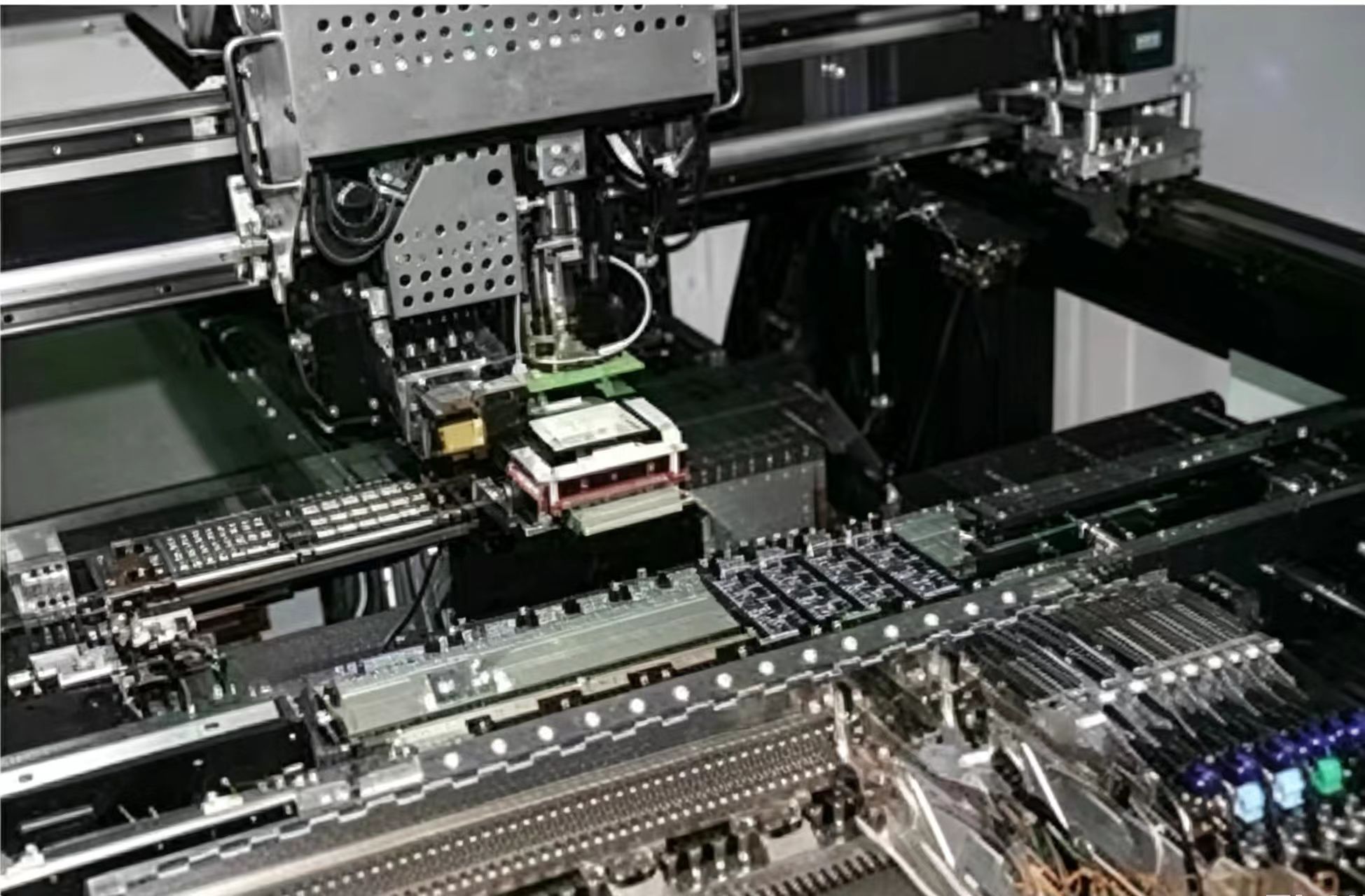
The details of the fiducial are what make it usable. A typical requirement is a contrast ratio between the mark and the surrounding laminate, with no other pads, paste or silkscreen within about 2 mm of the mark edge, because anything that changes the shape or the contrast can be misidentified. A fiducial patterned with thin lines rather than a solid shape cannot be recognised reliably, and a highly reflective finish can saturate the camera. Plating the mark to control its appearance is a common and inexpensive fix.
Edge Clearance and Panelization
The conveyor holds the board along its long edges, and the placement machine cannot place parts within that band. A 5 mm strip along each long edge should therefore be kept free of surface mount components. If the circuit cannot spare the area, a breakaway process edge is added to the panel and removed after assembly.
The recommendation is to keep the restriction on the component side of the board rather than on the solder side where possible, and to apply it to the long edges of the panel rather than to each individual board. Panelization itself is a manufacturing decision, and the panel and placement layout should be confirmed with the assembly house before the artwork is released.
Pads, Vias and Thermal Relief
Placing a via directly in a solder pad is one of the most common design errors. During reflow the paste wicks into the via, which leaves the joint short of solder and produces a weak or open connection. Vias should be placed beside the pad and connected with a short trace, or filled and plated over if the density demands it.
The second pad-related issue is heat. A pad connected directly to a large copper pour or plane conducts heat away faster than the solder can melt, which produces incomplete melting and a cold joint. Thermal relief spokes slow the heat flow enough for the joint to form, and they should be applied wherever a pad is connected to a plane, especially on boards with large ground areas.
Silkscreen, Polarity and Identification
Silkscreen exists to prevent mistakes. Polarity of diodes, tantalum capacitors and electrolytic capacitors should be marked in the conventional way, so an operator or an inspector can verify orientation without referring to the data sheet. Where an assembly house is working from a placement file, the marking is the last line of defence against an incorrect rotation in the program.
Legibility matters as much as presence. Small characters, characters placed over vias and characters that overlap pads make the board harder to inspect. Part numbers are best hidden, especially on dense boards, while reference designators must be visible, because the placement program is generated from the designators and an inspector needs to match components to the BOM.

Component orientation and spacing are the next group, and they interact with the machinery itself.
Component Orientation and Spacing
Placement machines rotate nozzles in fixed increments, typically 90 degrees, so a component placed at an arbitrary angle will be offset by the difference between the required angle and the achievable one. Keeping rotations to the four cardinal directions removes that error entirely.
Tall components should not be placed directly next to each other. The nozzle needs clearance to place the second component, and if the first one is in the way the machine detects the collision and stops, which costs production time and may require a program change. Where the height cannot be avoided, spacing the parts or reordering the placement sequence is the answer.
Small components under large ones create a different problem. Placing resistors under a display, for example, means that the display must be removed before the resistor can be reworked, and removing the display may damage it. Moving the small parts to the opposite side of the board costs nothing and preserves rework access. The order of placement and pad positioning is worth reviewing with the assembly house at the same time.
Footprint Dimensions for Machine and Hand Soldering
For packages such as small outline, plastic leaded chip carrier and quad flat pack, the pad length should be about 1.5 times the length of the component lead. A longer pad gives the solder a place to form a fillet, which helps both machine soldering and hand soldering with an iron. The pad width should match the nominal lead width from the data sheet rather than being widened for convenience, because widening it reduces the gap between adjacent pads and encourages solder bridging between them.
Where adjacent pins are intentionally connected, the connection should be made through a short external link covered by solder mask rather than by a large exposed copper shape. This keeps the joint inspectable and avoids an unintended bridge forming elsewhere on the same row.
BGA packages need provision for rework. Adding two locating holes of around 30 mil near the package lets a rework stencil be aligned over the site, which makes reballing or reflowing the part practical instead of a gamble. The holes should be sized so that the alignment pins fit snugly without play.
Colour and Other Practical Details
Solder mask colour is not purely cosmetic. Some machine vision systems illuminate the board with red light, and a red mask appears white under that illumination, which removes the contrast the camera needs. Choosing a different mask colour removes a problem that has nothing to do with the electrical design.
Finally, the panel and the process edge should be defined together with everything above. Their dimensions decide the conveyor handling, the breakaway method and the space available for fiducials, and they are much easier to agree at the start of the project than to retrofit afterwards. The broader set of PCB design guidelines for manufacturability provides the context for all of these checks.
FAQ
How big should a fiducial mark be? A copper dot of about 1 mm diameter with a clear area of roughly 2 to 3 mm around it is a common requirement. The important properties are contrast, a solid shape and a keep-out that excludes pads, paste and silkscreen.
Why is a via in a pad a problem? The paste wicks into the barrel during reflow, so the joint is short of solder. If the via must be in the pad, it should be filled and plated over rather than left open.
Does solder mask colour affect assembly? It can. Under the red illumination used by some vision systems, a red mask loses contrast. Other colours are safer where machine vision is used for programming and inspection.