




PCB Design Guidelines That Make Boards Manufacturable
Most layout mistakes are not made because the rules are unknown. They are made because the rules are applied only to the parts of the board that the designer is thinking about at the time, and the rest is drawn by habit. Guidelines exist to make the application uniform, and the six below are the ones that repay the effort most reliably.
Component Arrangement Comes First
Placement should be developed in stages and reviewed between them, rather than adjusted continuously while routing. The first stage fixes the mechanical parts; the second places the core device and the power section; the third groups the analog, clock and interface circuits; the last fills in the passives that support the devices already placed.
The reason for the sequence is that each stage defines the constraints for the next. A designer who places everything at once and then adjusts placement during routing is effectively routing twice. Grouping components by function also reduces the length of the connections inside each group, which improves both signal behaviour and the ease of routing. The order itself is described in this article on placement order and pad positioning.
Routing Rules Applied Uniformly
Trace width should be set from the current and the impedance requirement rather than from a default. Spacing should follow from the crosstalk that can be tolerated, with the sensitive nets given the additional separation they need. Corners should be at 45 degrees rather than at right or acute angles, and the routing should avoid unnecessary layer changes on fast nets.
The point of uniformity is that a design cannot be reviewed against rules that were applied inconsistently. Where a width or a spacing has to deviate, the deviation should be deliberate and recorded, so that the reviewer knows it is intentional rather than accidental. The routing geometry that produces the best results is described in this discussion of PCB routing and impedance control.
Thermal Reliefs and Copper Balance
A thermal relief is a connection between a pad and a plane that reduces the amount of copper attached to the pad while maintaining a thermal path. Its purpose is to let the pad reach soldering temperature at roughly the same rate as the pads around it, so that the component does not shift or tombstone during reflow.
The width of a thermal relief spoke is a design decision with an assembly consequence. Spokes that are too narrow restrict the current path and produce a local hot spot; spokes that are too wide defeat the purpose by making the pad behave as though it were fully connected to the plane. The dimensional relationships involved, including the pad and hole sizes that the relief connects, are set out in this article on PCB pad design standards.
Silkscreen, Mask and Documentation Practice
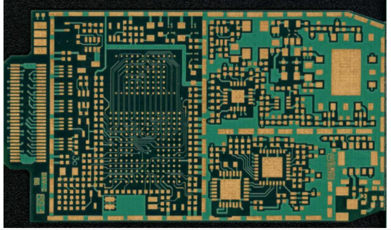
The silkscreen should identify every component, its orientation and its reference designator, and it must not overlap a pad that will be soldered. A silkscreen printed across an aperture interferes with the paste deposit and can leave ink in the joint. Reference designators should be placed so they remain legible after assembly, which means they should not be hidden under a component body.
The solder mask openings follow the pads, with a defined expansion that the fabricator applies. Where a design needs a mask dam between two pads, the dam width must be within the printing capability, and where it is marginal the ink behaviour becomes the limiting factor rather than the copper geometry.
Design Review as a Habit
A design review that happens once, at the end, finds problems when they are expensive. The same review applied in stages, after placement, after power routing, after signal routing and before release, finds the same problems while they are cheap. The checklist should be specific to the organisation and it should reference the actual limits of the fabricator being used rather than a generic specification.
Review is also the mechanism by which the guidelines stay current. When a problem is found in production, the correction belongs in the checklist as well as in the design, so that the same mistake is not repeated on the next project. That habit is what turns a set of rules into a process.
Manufacturing Feedback
The last guideline is to keep the fabricator in the loop. A design that has been reviewed against a specific supplier capability is different from one that has not, and the difference is visible in the questions that do or do not arise during fabrication. Where a design pushes a limit deliberately, the reason should be recorded so that the fabricator does not silently adjust the artwork. The reporting of those adjustments, and the reasons they occur, is described in this discussion of PCB design and fabrication.
Trace Routing Widths and Current
Trace routing is where the guidelines meet the arithmetic. A power trace has to satisfy a temperature criterion and a voltage drop criterion, and the smaller of the two sets the width. A signal trace has to satisfy an impedance target if it is fast, and a spacing requirement if its neighbour is noisy. Applying those rules uniformly means calculating the width once per net class and then using that value everywhere the class appears, rather than making an individual judgement at each trace.
Where a net has to change width, the change should be made where the impedance matters least and it should be gradual. A trace that narrows abruptly to pass between two pads creates a local hot spot as well as a reflection, and both effects are avoidable by routing the narrow section where the current is low or the signal is slow. Vias are part of the same calculation, since a path that passes through several of them has resistance contributed by each, and the rules for sizing those holes are described in this discussion of via to trace clearance.
Guidelines and Review Discipline
A guideline is only useful if it is applied before the layout is complete. The habit that makes it work is to review the design against the checklist at the end of each stage, when the geometry is still fluid and a correction costs minutes rather than hours. A design reviewed only at the end of the layout will be reviewed against a finished structure, and the changes that come out of that review are the expensive kind.
It also helps to keep the checklist short and specific. Ten items that are always checked are worth more than a hundred items that are consulted occasionally, particularly when the items reflect failures that have actually occurred on previous projects rather than a generic list of advice.
FAQ
Which guideline matters most? Placement, because it determines the length of every connection and the geometry that every later decision depends on. A board with excellent routing built on poor placement is always worse than the reverse, and placement errors cannot be corrected by adding effort later.
Why does a thermal relief have to be sized carefully? Because it controls the balance between the thermal path and the copper area connected to a pad. Too little copper and the pad runs hot; too much and the pad heats more slowly than its neighbours, which shifts the component during reflow.
How often should a design be reviewed? At each stage rather than once at the end. A review after placement catches mechanical and thermal problems, a review after power routing catches distribution problems, and a final review before release catches documentation and output errors.


2 Comments
BOM for SMT Prototype Assembly: A Practical Checklist
[…] A short checklist before release catches most of them: every designator appears exactly once, every part number resolves to a real orderable item, every package matches the board footprint, and every line has a quantity and a unit of measure. Checking a BOM against that list takes minutes and prevents most delays. Further guidance on preparing manufacturable output is available in these PCB design guidelines for manufacturability. […]
Additive Process in PCB Manufacturing: Design Notes
[…] Because an unmarked hole may still receive mask by default, every hole should be declared explicitly in the design data with its requirement. If a hole is intended to remain open, that should be stated; if it is intended to be covered, that should be stated too. Leaving the question to a default is what produces ink on the table and an unplanned interruption in the shop, and it also produces a board whose vias behave differently from the design intent. This is a small documentation habit with a measurable effect on delivery, and it belongs in the same set of habits as the general manufacturability rules described in this article on PCB design guidelines that keep a board manufacturable. […]