Debugging Power Supply Noise and Clock Coupling in Measurement Circuits
Precision analog circuits fail in ways that a schematic review will never reveal. A 16 bit measurement channel can meet every specification on paper and still return noisy data, because the noise enters through the power pins, through a clock trace that runs too close to a high impedance node, or through an amplifier that is driven beyond its linear range. Finding the source is a matter of method rather than guesswork.
Start With the Power Supply
Most unexplained noise in a measurement circuit arrives through the supply pins of the active devices. A switching regulator that powers an instrumentation amplifier, a voltage reference and an analog to digital converter will inject its switching residue into all three unless the impedance between the supply and the device is low across the switching frequency and its harmonics.
The evidence is easy to see. Take a long record of converter output with the input held at a fixed, clean reference, and look at the histogram. A wide, roughly Gaussian distribution with no structure points to random noise, while a distribution with shoulders or repeated levels points to a coherent interfering signal that is being sampled along with the measurement.
The measurement itself has to be trustworthy before any conclusion is drawn. The reference should be a clean DC source, the converter should be clocked from a source that is not shared with the switching regulator, and the record should be long enough for the histogram to settle. A short capture can look clean by accident, and a reference that is itself noisy hides the very effect being hunted.
Bypass Capacitor Placement and Mix
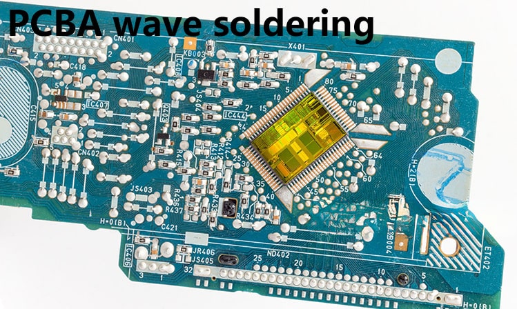
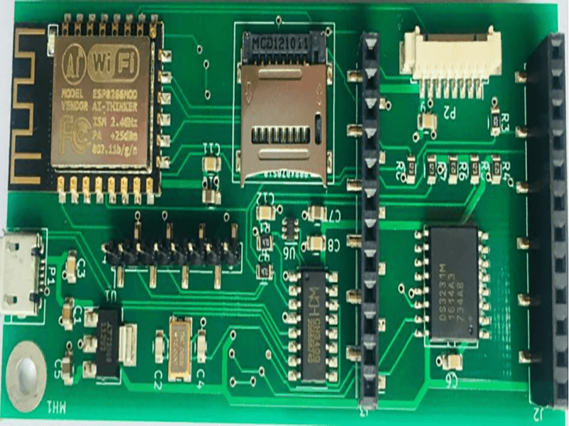
The fix is a combination of capacitor values placed at the right physical location. One bulk capacitor of about 10 microfarads handles the low frequency demand, and several small ceramic bypass capacitor parts of 0.1 microfarad placed as close as possible to each supply pin handle the fast edge currents. The small parts must be closer to the pin than the bulk part, because the trace inductance between the capacitor and the pin is what defeats them at high frequency.
The distinction matters because the remedies are different. If the harmonic family moves when the gain is reduced, the problem is headroom. If the harmonics stay at the same frequencies as the input level changes, the distortion comes from elsewhere in the signal chain, and the next candidate is the reference or the converter drive circuit.
Placement is the whole point. A 0.1 microfarad capacitor placed 10 mm from the pin is electrically invisible at the frequencies that matter, because the loop area formed by the capacitor, the trace and the ground path adds more inductance than the capacitor removes. Where a via is needed to reach the ground plane, the capacitor should share the via with the pin wherever the layout allows, so that the return current does not have to find a separate path.
The capacitor dielectric matters as much as the value. A small case size with a stable dielectric holds its capacitance at the switching frequency and over temperature, while a large case part may lose most of its value under DC bias. Two well chosen components usually outperform one large one.
Clock Coupling Into Analog Traces
Digital clocks are the second common source. A clock trace that runs parallel to a high impedance analog trace will couple into it capacitively, and because the coupling is not related to the conversion process, the interference appears as spikes rather than as random noise. A square wave couples through its harmonics, so the interference is spread across the spectrum rather than confined to one frequency.
Two remedies work together. The analog trace should be moved away from the switching trace, or routed on a different layer with a ground plane between them, and an anti aliasing filter ahead of the converter should be placed as close to the input as possible. Where the coupling is random rather than periodic, frequency domain analysis is less useful and a time domain record of the analog input is the better tool. The layout measures that reduce this class of coupling are described in the notes on mixed signal PCB design guidelines.
Distance is the cheapest fix and shielding is the next. Doubling the separation between the aggressor and the victim reduces the coupling, and routing the two on different layers with a solid reference plane between them removes it almost entirely, provided the return currents do not share a region of the plane.
Amplifier Overdrive and Distortion
A third source is not noise at all. When an amplifier is driven slightly beyond its linear range, the output compresses and the distortion products appear as harmonics of the input signal. On a spectrum plot the fundamental looks broadened and a family of harmonics rises out of the noise floor at multiples of the input frequency. The circuit is functioning, but the gain is set too high for the signal being applied.
Reducing the gain restores linearity, and the harmonics collapse. The diagnostic value is that the harmonic family identifies the mechanism immediately: evenly spaced lines at multiples of the stimulus frequency are distortion, while lines at the clock frequency and its multiples are coupling.
Three Tools, Three Questions
Three measurements answer almost every noise question. The histogram is a direct current analysis: it shows the distribution of the converted codes and reveals whether the noise is random or has structure. The fast Fourier transform is a frequency domain analysis: it separates the noise into components and shows the frequency of anything coherent, which usually identifies the source by inspection. The oscilloscope is a time domain analysis: it shows whether the disturbance is a spike, a step or a continuous waveform, and how it relates in time to other events in the system.
Documenting each measurement is what turns a one-off fix into a design rule. When a clock coupling problem is traced to a specific pair of traces, the finding belongs in the layout guidelines for the next board, together with the spacing that resolved it. Teams that record these outcomes stop rediscovering the same coupling mechanism on every product.
Using all three together is what makes the diagnosis fast. A histogram with structure sends you to the spectrum plot, the spectrum plot names a frequency, and the oscilloscope confirms where that frequency is coming from. Ground return problems deserve a separate look because they disturb all three measurements at once, and the mechanisms are described in the notes on ground current and harmonic distortion and in ground routing and power trace planning.
Several habits remove most of these problems before they appear. Analog and digital sections are kept physically separate with a single defined crossing point, high impedance nodes are kept short and away from switching nets, and the return path for every signal is continuous from source to load.
Component selection supports the layout. A converter with a well specified reference input and a low noise regulator removes problems that no amount of routing can fix, and a precision reference is wasted if it shares a supply rail with the digital section.
Finally, the grounding scheme deserves a deliberate decision rather than a default. A single continuous ground plane with one defined crossing point between the analog and digital areas usually outperforms a plane that has been cut in two, because a split plane forces return currents to detour and creates the very loop that the split was meant to prevent.
Documenting each measurement is what turns a one-off fix into a design rule. When a clock coupling problem is traced to a specific pair of traces, the finding belongs in the layout guidelines for the next board, together with the spacing that resolved it. Teams that record these outcomes stop rediscovering the same coupling mechanism on every product.
Debugging Power Supply Noise with FFT Analysis
When a prototype fails EMC or shows jitter on clock lines, the first suspect is often power supply noise rather than the signal path itself. Probing the rail with a low-inductance ground spring and a DC-coupled scope input isolates ripple from switching transients, and the shape of the waveform usually points at the culprit before any schematic change is made.
Capturing the same rail with FFT analysis turns that waveform into a spectrum, and the peaks line up with switching harmonics, diode recovery edges or a resonance between the bulk capacitor and the trace inductance. Moving a decoupling capacitor closer to the load, or splitting the plane under the analog section, typically drops the peak by 10 to 15 dB without adding any component cost.
Record the spectrum before and after each change. A baseline file keeps the debug honest and shows reviewers exactly which modification removed the emission, which matters when the same fix has to be justified for a production release.
FAQ
How large should the bypass capacitors be on an analog supply pin? A 0.1 microfarad ceramic part at each pin, backed by one bulk capacitor of about 10 microfarads for the whole supply rail.
Why does a clock trace cause noise on a DC measurement? The clock couples capacitively into the analog trace, and its harmonics are sampled by the converter along with the signal.
Is a histogram or an FFT better for finding noise? They answer different questions. The histogram shows whether the noise is random or coherent, and the FFT identifies the frequency of a coherent component.