Mobile Phone PCB: Design and Construction
A phone board is the most demanding consumer circuit board in volume production. It carries a processor, a radio, a power management system, cameras, display and audio in a volume smaller than a credit card, and it has to survive being dropped. Almost every technique used in high density design appears on it at once.
How Many Layers and Why
Current phone main boards use ten or twelve layers, and the count is driven by the escape routing from the processor and the number of supply rails rather than by the number of components. A ball grid array with a fine pitch can only be escaped if there are enough inner layers to route the signals away.
Each added layer costs lamination cycles and yield, so the count is pushed as low as the routing permits. That pressure is what drives the use of finer lines and smaller vias, which in turn requires the HDI construction described below. Our layer assignment article describes how the arrangement is planned.
HDI Construction
A phone board is built as an HDI stack: fine lines and spaces on the outer layers, laser drilled microvias between adjacent layers, and thicker conventional layers in the core. The microvias allow connections where a through hole would consume too much routing space.
The construction is sequential, meaning layers are added in stages with drilling and plating between them. That is what makes the board expensive, and it is also what makes the density possible. Our blind and buried via article describes the process steps involved.
Miniaturisation and Its Limits
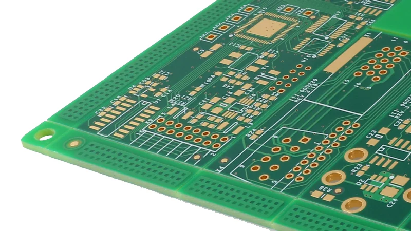
The components on a phone board are the smallest available in volume: 01005 chip parts, fine pitch packages and wafer level devices with no package body beyond the die. The board has to place and solder them reliably, which constrains the pad geometry and the stencil design.
The practical limit is the assembly process rather than the fabricator. Paste deposits below a certain volume do not release consistently, and placement accuracy has to be better than the pad tolerance allows for. Miniaturisation is therefore a joint decision between the layout, the stencil and the placement machine. Our stencil fabrication notes describe the printing side.
<img src="https://www.gopcba.com/wp-content/uploads/2026/08/SMT-PCB-Printed-Circuit-Board-Assembly.webp" alt="rigid flex assembly inside a mobile phone housing” />
Thermal Constraints in a Sealed Volume
A phone has no fan and almost no free volume, so all the heat generated inside has to leave through the case. The board’s role is to spread heat from the processor and the power amplifier into the largest available area, and from there into the metal frame or the back cover.
That makes the internal copper planes part of the thermal design rather than only the electrical design. Thermal vias beneath the processor connect to planes that spread the heat laterally, and the mechanical path from the board to the case is as important as anything on the board itself. Our thermal management article describes the general approach.
Rigid Flex and Antenna Integration
Many phones use a rigid flex assembly in which the main board connects to a daughter board or a connector panel through a flexible section. The flexible portion removes a connector and its assembly step, and it allows the two rigid sections to sit in different planes.
Antennas are increasingly formed as patterns on the board itself or on a flexible extension, which makes the board a radio component as well as a carrier. That changes the layout requirements, because the antenna area must be kept clear of copper and of conductive components.
Mechanical Durability
A phone is dropped, sat on and flexed. The board has to survive that, and the failure mode of interest is a cracked solder joint or a cracked component rather than a broken board.
Designing for it means keeping large components away from the areas of the board that flex, avoiding placing heavy parts at the midspan of an unsupported region, and using underfill where a large package must be placed near a flexing area. Our component tolerance and reliability notes describe how that strain is estimated.
Design Constraints Worth Checking
The constraints on a phone board are numerous and they interact, which is why they are usually tracked as a checklist rather than addressed one at a time. The following are the ones that most often force a layout change late in a project:
- Confirm the escape from the processor package is possible on the planned layer count before routing begins.
- Check that every supply rail has a plane or a wide enough path to the device that uses it.
- Confirm the fine line and space capability against the fabricator the board will actually be built at.
- Verify that microvia stacking is permitted by the construction and by the fabricator capability.
- Check that the antenna area is clear of copper, components and coatings that change its behaviour.
- Confirm the thermal path from the processor to the case through planes, vias and mechanical contact.
- Check component placement against the areas that will flex during drop and during normal use.
- Confirm the flexible section of a rigid flex assembly respects the bend radius at every position it will occupy.
- Verify that test access exists for the nets that cannot be covered by functional test.
- Confirm that the assembly process can place and inspect the smallest parts on the board.
Each of these has been the reason for a late redesign on some product, and each costs nothing to check before the layout is finalised. Our design release checklist places them in the review sequence.
Material and Surface Finish Choices
Mobile phone boards are overwhelmingly built on FR-4 with a Tg of at least 150 °C, and many high-volume designs now use halogen-free laminates to satisfy regional substance regulations. The surface finish matters just as much as the laminate. Electroless nickel immersion gold gives a flat, solderable pad that survives repeated reflow and is the usual choice where fine-pitch components and long shelf life are required, while immersion silver offers a lower-cost alternative with excellent wettability but a shorter storage window. Organic solderability preservatives remain popular on cost-driven boards because they add almost nothing to the bill of materials, though they tolerate only a limited number of heat cycles. Whichever finish is specified, the copper beneath it should be a minimum of one ounce per square foot on the outer layers, because thin foil etches unevenly and produces impedance variation that shows up later as signal integrity problems on high-speed traces.
Testing and Quality Control
Every panel passes through automated optical inspection after etching to catch opens, shorts and nicks before any components are placed. Electrical test follows, using a flying probe or a dedicated bed-of-nails fixture, and it verifies continuity and isolation on every net rather than sampling. For boards that carry radio frequency circuitry, impedance coupons are built into the panel border and measured with time-domain reflectometry so the fabricator can confirm that the controlled-impedance traces land within tolerance. Finally, a solderability test on a sample from each lot confirms that the finish has survived storage and handling. These steps add cost, but they are the reason a phone that has been dropped, heated in a pocket and charged a thousand times still boots. Working with a fabricator that documents each of these checks, and that can share the coupon data on request, is worth far more than shaving a few cents from the unit price.
FAQ
Why do phone boards need so many layers? Because the escape routing from fine pitch packages and the number of separate supply rails both demand routing space that the outer layers cannot provide.
What is an HDI board? A board built with fine lines and laser drilled microvias, usually in a sequential build, to achieve routing density that conventional multilayer construction cannot reach.
Is a phone board flexible? The main board is rigid. Many phones use a rigid flex assembly where the flexible portion handles the connection between rigid sections.
How is heat removed without a fan? Through copper planes and thermal vias into the board, and from the board into the frame and the case. The board is part of the thermal path rather than merely a carrier.
What limits how small the components can be? The assembly process. Paste release and placement accuracy set a floor, and the layout has to work within it.