Flexible PCB Coverlay: Materials, Openings and Defects
A coverlay is the flexible circuit equivalent of solder mask, but it does much more than a mask. It is a laminated layer of polyimide with an adhesive that is pressed over the finished conductors, protecting them from contamination and mechanical damage, defining which areas remain exposed for soldering, and contributing to the mechanical behaviour of the part. Getting the coverlay right is one of the less visible but more consequential parts of a flexible circuit design.
This article covers the material options, how openings are defined, what happens to the adhesive during lamination, and the defects that appear when the design and the process disagree.
What a Coverlay Is Made Of
A typical polyimide coverlay is a film of 12.5 to 25 microns, coated with a layer of acrylic or epoxy adhesive. The film provides the electrical and mechanical protection, while the adhesive bonds it to the flex. Total thickness of a standard coverlay is usually between 25 and 75 microns, and that thickness enters every mechanical calculation for the part.
The alternative is a photo-imageable coverlay, which is applied as a liquid or a dry film and patterned like a solder mask. It avoids the separate die-cutting step and can hold finer openings than a laminated coverlay, but its dielectric and mechanical properties are different and it is less suitable for dynamic flexing applications.

Adhesive Systems and Their Behaviour
The adhesive is the part of the coverlay that causes most of the problems. During lamination it softens and flows, filling the space around the conductors and bonding to the polyimide beneath. If it flows too far, it creeps into an opening and covers a pad; if it does not flow enough, voids remain under the film and delamination follows.
Adhesiveless coverlays eliminate the adhesive by bonding the film directly to the base material. The result is thinner, more dimensionally stable and better in dynamic bending, at a higher material cost. Where the flex will move repeatedly in service, the thinner stack is worth the premium, because a coverlay that is thinner reduces the strain on the outermost copper.
<img src="https://www.gopcba.com/wp-content/uploads/2026/05/SPI.jpg" alt="Coverlay opening exposing pads on a flexible circuit” />
Defining the Openings
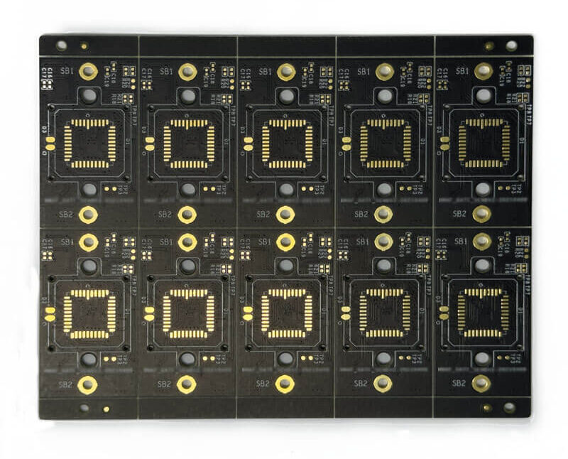
Each opening in the coverlay is a window that exposes a pad, a test point or a connector area for soldering. The opening is cut slightly larger than the pad, because the adhesive will flow inward during lamination and reduce the effective opening. The amount of this allowance depends on the adhesive type and on the pad geometry, and a common starting point is 0.1 to 0.2 mm on each side.
The pad itself has to account for the same effect. A pad that is too small will be partially covered after the adhesive flows, leaving a land that is difficult to solder and that may not form a proper fillet. Standard pad geometry rules still apply, but the annular ring on a flexible circuit must be generous enough to absorb the coverlay registration tolerance.
Registration and Tolerance
Coverlay lamination involves registering a die-cut film to the patterned conductors, and that registration is less precise than the imaging of a solder mask. Typical tolerances are a few tenths of a millimetre, and the effect is that the position of the opening relative to the pad varies from part to part.
The design has to absorb that variation. Conductor traces should not run close to the edge of an opening, and the exposed pad should be large enough that the opening can move without exposing the conductor beneath. Where the opening also has to clear a connector boss or a housing feature, the mechanical tolerance is added to the registration tolerance.
Coverlay and the Bend Area
In a dynamic bend area the coverlay is not a passive protection layer; it is part of the mechanical structure. The neutral axis of the bent stack depends on the thickness of the film and the adhesive on both sides, and an asymmetric build places more strain on one side of the conductors.
Balanced construction is therefore the rule. The coverlay on the component side and the base and coverlay on the other side should give a stack in which the copper lies close to the neutral axis. Where the flex is formed once during assembly, the requirement is much less exacting, and a standard coverlay is entirely adequate.
Common Defects
The most common defect is adhesive squeeze-out into an opening, which leaves solderable areas partly covered. It appears as a thin, glossy film over the pad that prevents wetting, and it is usually a consequence of excessive lamination pressure or a pad that is too close to the opening edge.
The second is delamination, which shows as a blister or as a lifting edge after thermal cycling. It is caused by trapped moisture, contamination on the polyimide surface before lamination, or insufficient bonding pressure. The third is cracking of the coverlay itself in a tight bend, which is a geometry problem rather than a material one, and the answer is a larger bend radius.
Surface preparation decides whether the bond survives at all. Polyimide is chemically inert, and an adhesive will not key to a surface that still carries release agent, oxide or handling contamination. Most flex lines therefore treat the surface before lamination with a plasma or a chemical etch, and the treatment has to be completed within a limited window before the coverlay is applied. Where adhesion problems recur on one part of a panel, the treatment step is usually the place to look first.
Design Rules to Follow
Keep the coverlay openings simple in shape, with rounded corners rather than sharp internal angles, and keep them clear of the bend area. Allow for the adhesive flow allowance on every pad, and give the coverlay enough room at the board outline so that the film can be cut cleanly. Where a stiffener is bonded to the flex, the FR4 stiffener placement rules interact with the coverlay, since both are laminated in the same area.
Where the flex is part of a rigid-flex construction, the coverlay has to stop short of the rigid section and the transition must be planned so the film does not extend into a region that will be laminated with prepreg. Getting the outline and the openings right at the design stage, as the flexible circuit outline guidance describes, avoids a rework cycle at the fabricator.
FAQ
Can a coverlay opening be smaller than the pad? No. The opening is always larger than the pad, because the adhesive flows inward during lamination and the registration tolerance has to be absorbed. Making the opening smaller than the pad guarantees partial coverage after processing.
Is a coverlay always required? Not in every flex design. Where the conductors are on an inner layer of a multilayer flex, the outer layers protect them and no coverlay is needed in that area. Exposed conductor areas still need protection, either from a coverlay or from a coating.
How does a coverlay affect flexibility? It increases the total thickness of the flexible section, which raises the strain for a given bend radius. Using thin adhesiveless materials and keeping the stack balanced are the two ways to preserve flexibility while still protecting the conductors.