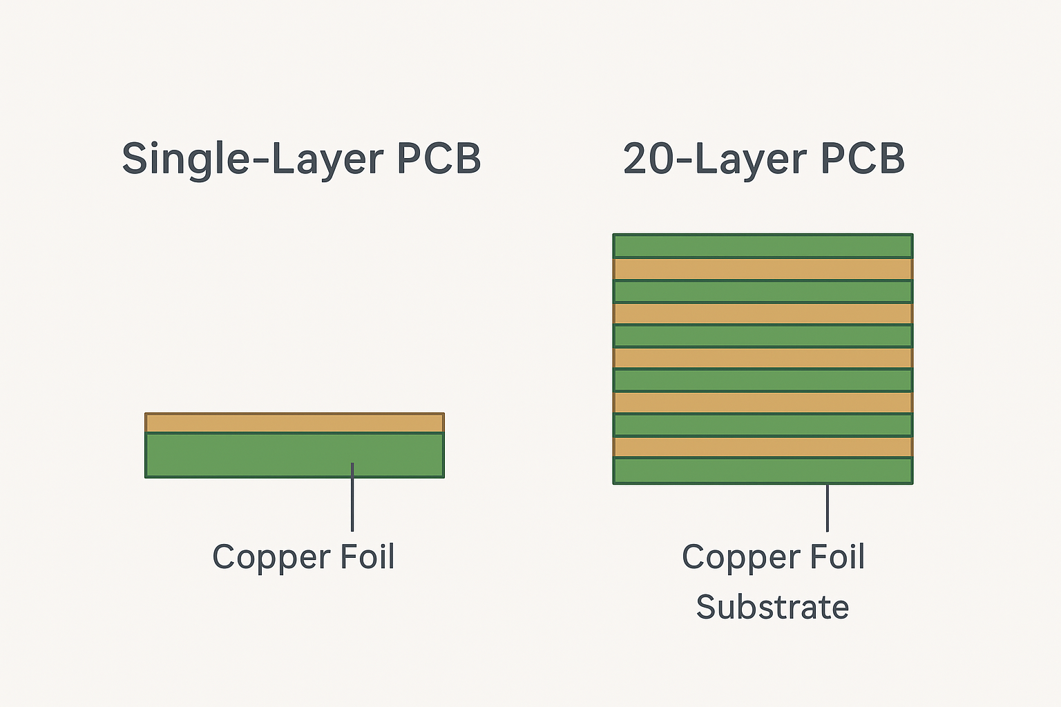
40-Layer PCB: Stack-Up, Materials and Process
A forty layer board is at the far end of what conventional laminated printed circuit technology can deliver, and it is built for one reason: an application needs so many connections between so many devices that no smaller stack can carry them. Backplanes for large switching systems, high channel count test equipment and specialised computing hardware live in this range. The design and fabrication problems that appear here are qualitatively different from those on a four or six layer board, and understanding them is the best way to see why layer count is only ever a symptom of the real requirement.
When a Stack Has to Grow This Far
Layer count is driven by the number of connections that must be routed between the devices, divided by the number that can be routed on each layer. A large backplane may have thousands of nets, each of which must run from one connector to another with a defined impedance and a controlled length, and the routing channels available between the connector pin fields are narrow. Increasing the layer count adds channels, and it also allows dedicated ground and power planes so that a reference plane is always available to the layers that need one.
The second driver is power distribution. A board of this size may carry dozens of supply rails, each needing a low impedance path to every device. Dedicated plane pairs give that path, and they also form the distributed capacitance that keeps the impedance low at high frequency. Above a certain size, the power distribution requirement alone can justify several layer pairs.
Stack-Up Planning and Symmetry
A stack of forty layers is planned from the middle outwards. The construction must be symmetric about the centre line, with the same sequence of copper weights and dielectric thicknesses on both halves, because an asymmetric stack will bow during lamination and stay bowed. It must also use a press schedule that the fabricator can actually achieve, which means the number of prepreg sheets and their resin content are chosen for the available press cycle rather than for electrical convenience.
The sequence of signal, ground and power layers follows the same logic as on a small board, applied repeatedly. High speed signal layers are placed adjacent to a reference plane, plane pairs are used for the supplies that need the lowest impedance, and layers that carry slow signals or static configuration are used as spacers where the geometry requires them. Our layer assignment notes describe how that arrangement is planned.

Lamination Cycles and Registration
No press laminates forty layers at once with acceptable registration. The board is built in stages, using sequential lamination: an inner core is laminated, drilled and plated, further layers are added, and the process repeats until the full stack exists. Each stage introduces its own registration error, and those errors accumulate, so the fabricator’s capability in this area is the single best predictor of whether a design can be built.
Sequential lamination is also where the cost lives. Each cycle consumes a press slot, requires its own drilling and plating steps and adds its own yield loss. A board that needs three cycles costs far more than one that needs two, which is why the design should minimise the number of blind and buried via stages even if that means accepting a slightly larger board area.
Aspect Ratio, Drilling and Back Drilling
A through hole in a thick board has a high aspect ratio, meaning the depth of the hole is many times its diameter. Plating a high aspect ratio hole evenly is difficult, because the plating solution must flow into a deep, narrow channel and exchange chemicals along its whole length. The practical limit depends on the fabricator’s plating line, and designs that exceed it must either use a larger hole, which consumes routing space, or accept a lower plating quality that will not survive thermal cycling. Our blind and buried via article describes the alternative where the ratio becomes unmanageable.
Back drilling addresses a different problem. A through hole that connects only the outer layers still has a barrel running through the rest of the board, and that unused portion is a stub that reflects energy and degrades the signal at high frequency. Back drilling removes the stub by re-drilling the hole to a controlled depth from the opposite side after plating. On a forty layer board the stub length would be enormous without it, so back drilling is standard on high speed signal vias in this class of product.
Materials and Process Control
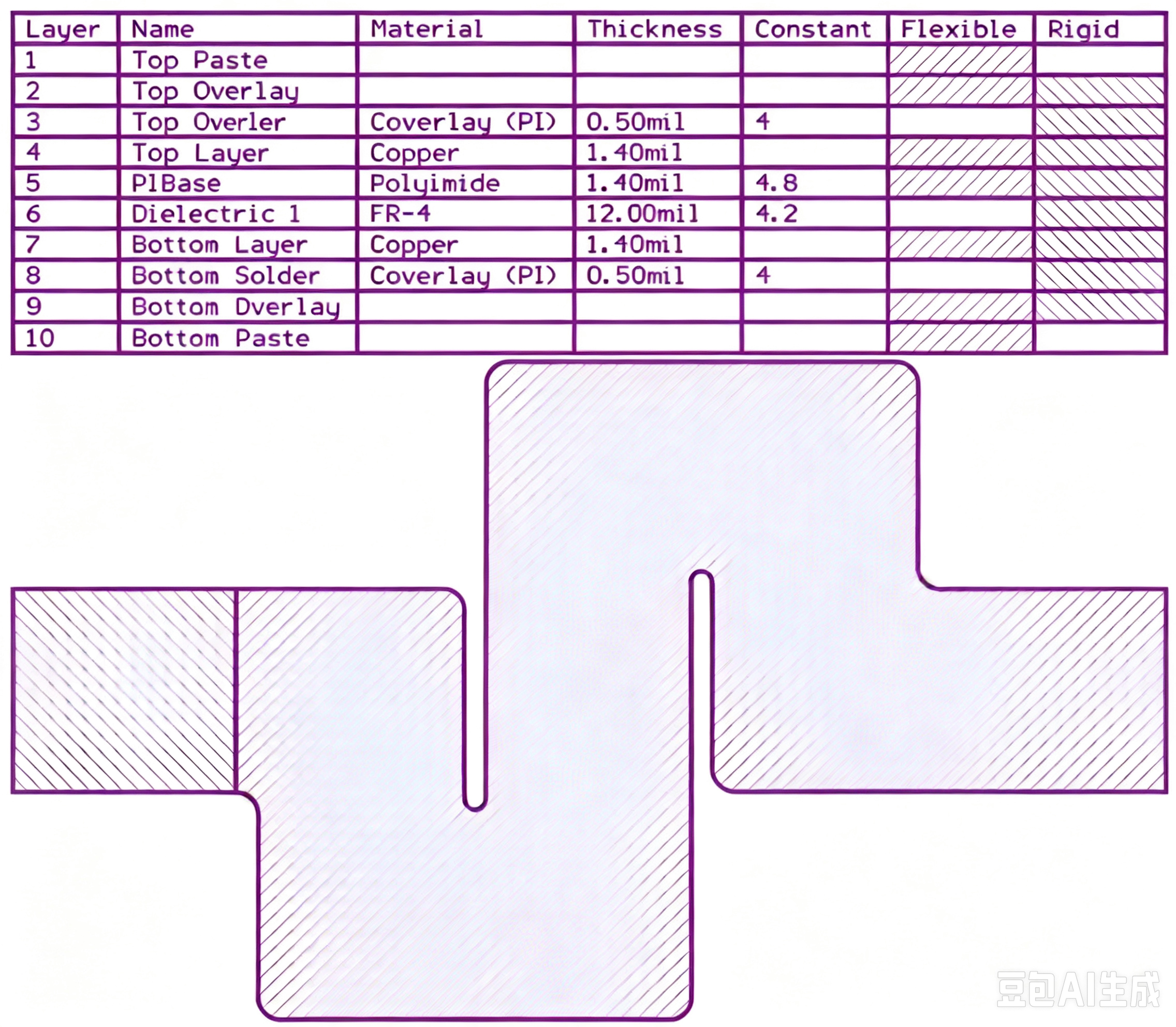
Thick stacks use dimensionally stable laminates, because a material that shrinks or expands unevenly during lamination will make registration impossible. Low flow prepregs are used to fill thick copper areas without leaving voids, and the copper weights are chosen so that each lamination cycle sees a balanced distribution. The materials are also selected for their behaviour after repeated press cycles rather than only for their electrical properties.
Process control is more demanding in every step. Drilling parameters are adjusted for the total depth, desmear has to reach the bottom of deep holes, and the plating bath must be monitored more frequently because the surface area of a thick board is far greater than that of a thin one. Panel thickness also changes how the board behaves in assembly: a thick board needs more thermal energy to reach reflow temperature and holds that energy longer, which affects the profile of every subsequent operation.
Testing a Very High Layer Count Board
Every net must be verified, and on a board with tens of thousands of nets a flying probe is impractically slow. A dedicated bed of nails fixture is used instead, with a test point on every net, and the fixture becomes a significant part of the project cost and lead time. Impedance coupons on the panel border are measured to confirm that the controlled impedance layers match the design values.
Cross sections are taken from a coupon on each panel and measured for plating thickness, layer registration and dielectric thickness, and the results are recorded rather than judged pass or fail. Where the product is a backplane that must work for a decade, the qualification programme also includes thermal cycling on a representative assembly, because the joints and the plated barrels in a thick board carry more strain than in a thin one. Our design release checklist covers the items that should be confirmed before a stack of this complexity is released.
FAQ
Is a forty layer board always better than a twenty layer board? No. More layers add routing channels and better power distribution at the cost of lamination cycles, registration risk and price. The right count is the lowest one that meets the routing, impedance and power requirements.
What is the maximum practical layer count? It depends on the fabricator’s press capacity, drilling depth capability and plating line, and it is usually expressed as a maximum aspect ratio rather than a layer number. Layer counts well beyond forty exist but are built by very few facilities.
Why is back drilling used on thick boards? A through hole leaves an unused length of plated barrel, and that stub reflects high frequency energy. On a thick board the stub would be long enough to ruin a fast signal, so it is drilled away to a controlled depth.