HDI PCB Prototyping: Microvia Stackup and Design Rules
HDI PCB prototyping is the stage where a dense design is proven on real laminate before tooling and volume commitments are made. A prototype run has to answer three questions at once: can the microvia stack be drilled and filled reliably, does the layer count still meet the routing demand, and does the stackup hold impedance targets across the whole board. Getting those answers early is cheaper than discovering them during a ramp.
What HDI PCB Prototyping Changes
A conventional multilayer board connects layers with mechanically drilled through holes. High density interconnect boards replace part of that with laser drilled microvias of much smaller diameter, built up layer by layer, which frees routing channels under fine pitch devices and shortens the return path for high speed nets. The prototype is where the fabricator proves that the chosen geometry can actually be produced.
Prototyping also settles the layer question. Many designs arrive with more layers than they need, or with too few and a routing crisis in the middle of layout. Building a small quantity first lets the team test the stack with real measurements instead of assumptions.
Microvia Types and Aspect Ratio
Microvias are usually defined as vias no larger than 150 µm in diameter with a depth-to-diameter ratio of about 1:1. A microvia that lands on the next layer only is a simple blind via; stacked microvias place one via directly on top of another, and staggered microvias offset them so the lower via is filled and capped first. Any-layer structures allow a via between almost any pair of adjacent layers.
Aspect ratio governs plating reliability. When the hole is too deep for its diameter, the plating solution cannot circulate properly and the barrel thins or voids at the bottom. Keeping the aspect ratio at or below 1:1 for laser drilled holes, and below 8:1 for mechanical through holes, avoids most plating risk. Where the design needs stacked vias, plan for copper filling and planarisation before the next build step. Comparing options in a blind and buried via stack selection review usually resolves the trade between density and cost.
Stackup Options: 1+N+1, 2+N+2 and Any-Layer
A 1+N+1 build adds one HDI layer above and below a conventional core. It is the cheapest way to gain routing density and covers most fine pitch escape requirements. A 2+N+2 build adds two layers per side, which gives more room for dense ball grid array fanout and better reference plane continuity for high speed signals.
Any-layer HDI removes the core entirely and stacks microvias freely, offering the highest density at the highest cost. Prototypes should use the simplest stackup that meets the routing and signal integrity requirement, because each additional buildup step multiplies process risk and lead time. Multilayer prototype requirements for impedance control and coupon design are covered in a separate note on multilayer prototype requirements.
Materials for a Fast HDI Prototype
High quality FR-4 satisfies most digital and industrial designs, especially when the highest signal rate stays below a few gigabits per second. The specification should still name the glass transition temperature, the decomposition temperature and the dielectric constant tolerance rather than leaving the grade open.
For fast serial links, low loss laminates reduce insertion loss and help close the eye at the receiver. They also press differently and may need adjusted drill parameters, so a prototype that uses them should be built with the material that production will use. Changing the laminate between prototype and volume is one of the most common causes of a failed second build.

Laser Drilling and Via Filling
Laser drilling removes dielectric with controlled energy pulses and stops on the underlying copper pad. Pad size, copper thickness and surface treatment all affect the process window, and a pad that is too small leaves no registration margin. Copper foil on the target layer should be thick enough to act as a stop but not so thick that it reflects unevenly.
Blind microvias are normally filled with copper plating or a conductive paste before the next lamination, so the surface stays flat for subsequent imaging. Plating quality at this step decides whether the finished via passes thermal cycling. The details are similar to those described for electroplating and via filling in HDI production.
Design Rules That Survive Fabrication
Minimum trace width and spacing on outer HDI layers are typically 75 µm and 75 µm, with inner layers slightly wider. Microvia pads generally need at least 250 µm of copper for reliable capture, and the capture pad on the target layer should be 50 to 75 µm larger than the via diameter.
Designers should also keep the number of sequential lamination cycles low, avoid via-in-pad without filling and plan the ground plane so that return currents are not forced through narrow necks. Every rule that saves process steps shortens the prototype schedule as much as it lowers cost.
Escape Routing and Fanout on HDI Prototypes
The payoff of a microvia stack shows up at the ball grid array. A dense array with a 0.4 mm pitch offers roughly 0.2 mm between pads, which is not enough for a trace to pass between them on a standard two layer escape. Microvias let the outer row drop to the next layer immediately, so the inner rows keep a clear channel outward instead of being blocked by their neighbours.
Fanout style decides how many layers are consumed. Dog-bone fanout costs almost nothing but eats routing space, via-in-pad with filled and capped vias saves space at the cost of extra plating and planarisation, and staggered microvias sit between the two. Plan the escape pattern before choosing the stack, not after the layout is finished.
Keep the reference plane intact under escaping differential pairs. A pair that crosses a plane split during escape will radiate and jitter even if the impedance coupon looks perfect, so route the pair on one layer and change reference only where a stitching capacitor sits nearby.
Quality Control on HDI Prototypes
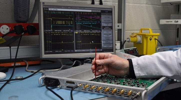
Inspection for an HDI build includes automated optical inspection after each imaging step, X-ray or cross section for microvia registration, and impedance coupons for controlled impedance nets. Thermal stress testing of a sample panel is the quickest way to expose weak plating in blind vias.
Documentation matters as much as measurement. The prototype report should record the actual dielectric thickness, the measured impedance, the via dimensions from a cross section and any deviation from the design rules, because that record becomes the baseline for the production build.
How to Shorten Prototype Lead Time
Send a complete fabrication package: Gerber data, drill and via schedule, stackup drawing, impedance requirements, surface finish and material specification. Incomplete data triggers questions that cost days. Ask for a DFM review before release, and resolve the findings in one pass rather than three.
Use standard materials and standard finishes where they are acceptable, keep the stack within a common build, and avoid unnecessary sequential lamination. Most schedule problems come from design choices rather than from the factory floor.
FAQ
Is a prototype stackup different from the production stackup? It should not be. The prototype exists to validate the stack that production will run, so changing layer count, laminate or via structure afterwards invalidates the result.
How many layers does an HDI prototype need? Use the fewest that support the routing and the reference planes. A 1+N+1 build handles most fine pitch escape problems, and only dense area array or high frequency designs justify 2+N+2 or any-layer.
Can laser drilled vias be inspected visually? No. Registration and plating quality are confirmed by cross section, X-ray or thermal stress testing, which is why the prototype report should include those measurements.