



Multilayer PCB Prototype Requirements Before Production
The prototype is the step where a design stops being a description and becomes an object. It is also the last inexpensive opportunity to find a problem: after the design enters volume production, every correction carries the cost of tooling, re-qualification and inventory. The requirements a multilayer prototype has to satisfy therefore cover more than the netlist, and they should be written down and checked rather than assumed.
Appearance and Dimensional Criteria
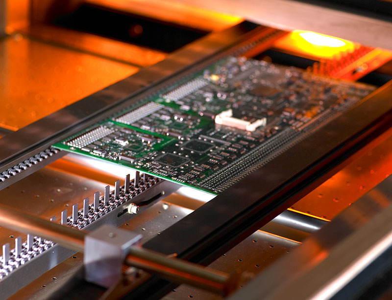
A prototype that will be assembled needs to be flat, free of burrs at the edges, and free of separation between the copper and the solder mask. The inspection should also cover copper that has been nicked by the routing operation, mask that has been damaged by handling, and any discolouration around a hole that would suggest plating contamination rather than a simple cosmetic mark. Those are not aesthetic conditions. A board that is not flat will not sit correctly on a stencil printer, which produces inconsistent paste deposits. A burr on an edge can interfere with a connector or a fixture. And lifting or blistering between the conductor and the mask is a bond failure that will grow.
These multilayer PCB prototype requirements are worth writing into the purchase specification, because a supplier who knows the appearance criteria in advance can build to them rather than discovering them at inspection. Moreover, the appearance criteria are only meaningful if they are measurable, so each one should reference a limit in a published acceptance standard rather than a description.
`r`n
The visual standard should be agreed with the fabricator in terms of a published acceptance specification rather than an impression. Copper that is exposed where it should be covered, mask that has run into a pad, plating that is discoloured and holes that are not fully plated are all detectable, and each has a defined limit. A prototype that fails any of them should be rejected before assembly rather than after.
A prototype that looks correct but measures incorrectly will fail at assembly, and the failure will appear in a fixture or an enclosure rather than on the board. Dimensional checks are equally important. The finished thickness, the board outline against the mechanical drawing, the diameter and position of mounting holes and the registration of the layers relative to each other all need to fall within tolerance, and the tolerance on layer registration is what determines whether the clearance rules were actually satisfied. That relationship is examined in this discussion of via to trace clearance.
Process Suitability and CAM Optimisation
A prototype also has to be manufacturable in the sense that its process window is real. If the design contains features that only work when every process is at its centre point, the prototype may succeed and the production run may fail. Checking the suitability of the design before the panel is built is therefore part of the prototype discipline, not an optional extra.
CAM optimisation is the step where the fabricator adjusts the data to fit the process. Line widths may be compensated for the etch factor, the spacing between traces and pads may be adjusted to satisfy the process minimum, and pad geometries may be trimmed to remove clearance violations. Those changes are normal and necessary, but they mean the board that is built is not identical to the data that was submitted.
The designer should therefore be told what was changed. A pad that was trimmed to satisfy a clearance rule is a pad with a smaller annular ring than the design intended, and a line width that was reduced to fit the process is a trace with higher resistance. Understanding how those adjustments are made helps the designer avoid the same violation next time, and the techniques are described in this article on HDI board CAM methods.
<img src="https://www.gopcba.com/wp-content/uploads/2026/08/PCB-assembly-on-bare-boards.jpg" alt="electrical test fixture checking a multilayer prototype panel” />
Electrical Test and Continuity Verification
An electrical test verifies that every net is continuous and that no two nets are shorted. For a multilayer board this is not a formality, because an open inside the board cannot be seen and a short between inner layers cannot be repaired. The test fixture must have access to every net, which means test points or vias must exist for each one, and the test coverage should be confirmed before the panel is built rather than after.
The test also needs to be appropriate for the geometry. A bed-of-nails fixture requires probe access on one side and adequate clearance between the probe targets. A flying probe test needs no fixture but takes longer per board. Where a net is accessible only through a via on the far side of a fine-pitch device, the fixture design may be the limiting factor rather than the electrical design.
What the Prototype Should Confirm
Speed is the reason prototypes exist, and the prototype requirements above are designed to keep that speed from turning into risk. The purpose of a prototype is to validate the assumptions the design made. Three of them are worth checking explicitly. First, that the stackup produces the impedance the design assumed, which can be verified on a test coupon built with the panel. Second, that the assembly process works on the actual geometry, including the smallest pitch and the largest thermal mass on the board. Third, that the clearances and dimensions the fabricator needs are satisfied across the whole panel, not just in the area that was inspected.
Designers who intend to move to volume production should also review the stackup at this point. A prototype stack chosen for availability may not be the stack that offers the best price at volume, and the rules that govern the choice are set out in this discussion of layer stackup design.
A Practical Checklist
Confirm that the outline and thickness are within tolerance, that the board is flat and free of burrs and delamination, that the mask registration is within the agreed limit, that every hole is plated correctly, that the electrical test covers every net, and that the CAM changes made by the fabricator have been reported. A prototype that passes all six of those checks is ready to be assembled, and the results give the production run a well-understood starting point.
FAQ
What should a multilayer prototype actually be checked for? Appearance and flatness, dimensional accuracy including thickness and outline, mask and plating quality, correct plating in every hole, and full electrical test coverage. Those checks can be performed before assembly, which is why they should be completed first.
Why does CAM optimisation change my design? Because the fabricator adjusts the data to fit the process, for example by compensating line widths for the etch factor or trimming pads to satisfy clearance rules. Those adjustments are normal, but they should be reported so the designer knows the geometry that was actually built.
Is electrical test enough to qualify a prototype? It verifies continuity and isolation, which is essential but not sufficient. It does not confirm impedance, assembly behaviour or dimensional accuracy, so it should be combined with the dimensional and process checks described above. A prototype that passes electrical test and nothing else has verified one assumption out of several, and the assumptions that remain unverified are the ones that appear as scrap in the production line.


4 Comments
PCBA Development Process Explained
[…] Some of that verification is analytical and some is empirical, and a prototype is what bridges the two. The purpose of the prototype is to test the assumptions the design made rather than to demonstrate that the circuit works, and the checks that a prototype should satisfy are described in this discussion of multilayer prototype requirements. […]
PCB Design Quality Characteristics
[…] Review is the mechanism that makes all of these characteristics real. A checklist applied progressively, as described in this discussion of multilayer design rules, catches problems while they are still cheap to fix, and the same discipline applies to the manufacturing outputs, whose requirements are set out in this article on multilayer prototype requirements. […]
PCB Design Release Checklist: DRC, DFM, Gerber and CAM
[…] Two problem classes deserve explicit checks because they are easy to introduce during last-minute edits. The first is grounding: any change to a split plane, a thermal relief, or a single-point ground connection should be recorded, because these modifications are difficult to spot later and can silently create a return-current discontinuity. The second is cutouts and openings: every window or slot in the board needs a routing keep-out so that a conductor cannot be trimmed into an open circuit during profile machining. Prototype runs are a good place to validate the whole workflow, as described in multilayer PCB prototype requirements. […]
Flexible PCB Materials: Polyimide, PET and LCP Compared
[…] that carries a high-speed link needs LCP or another low-loss film with a controlled dielectric. Multilayer PCB prototype requirements covers what the fabricator needs to build the first article from that […]