Imaging System PCB: A Complete Technical Guide
An imaging system is a measurement instrument that happens to produce a picture. Whether it is a medical scanner, a machine vision camera or a scientific detector, the board behind it has one job that dominates every other consideration: to preserve the signal against the noise the system itself generates. An imaging system PCB is therefore designed around a noise budget, and the layout decisions that follow are traceable back to that budget rather than to convention.
What the Board Has to Do
The signal chain starts at the detector and ends at a digital bus. A sensor converts the incident energy, whether light, X-rays or electrons, into charge or current. That charge is collected, converted to a voltage, amplified, filtered and digitised. Each of those stages adds noise, and the total determines the smallest feature the system can resolve.
The board also has to supply very stable voltages to the sensor and the converter, provide clocks with low jitter, and often control a mechanical or optical element. Those functions are not part of the signal chain, but their imperfection shows up in the image as fixed pattern noise, as banding or as a shifting baseline, and fixed pattern noise is the hardest kind to remove after the fact.
The Noise Budget and Where It Comes From
Noise enters at four points. The sensor itself has shot noise and dark current; the front end amplifier contributes its own voltage and current noise; the conversion adds quantisation and reference noise; and the power supply couples into all of them. The last of those is the one the board designer controls most directly, and it is frequently the one that limits a design that otherwise looked comfortable on paper.
Coupling is a layout problem before it is a component problem. A switching regulator two centimetres from a high impedance node will inject its switching frequency into the signal regardless of how good the regulator is, and the injection path is usually the reference or the ground rather than a direct radiated field. Keeping the analogue reference on its own quiet copper, and ensuring that the digital return current does not flow through it, removes most of the coupling. Our component tolerance and reliability notes describe how that error budget is assessed.
Sensor Interface and Readout
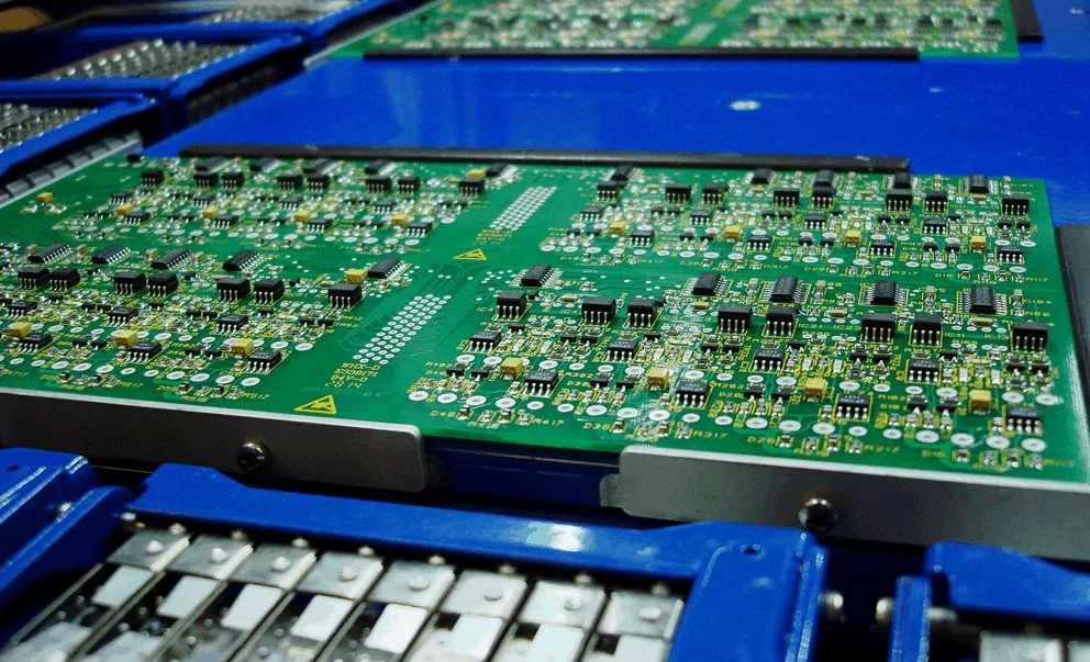
How the sensor is read depends on its technology. A charge coupled device transfers charge along a shift register and produces a sequence of packets that must be amplified with a correlated double sampling arrangement, which measures the reset level as well as the signal level and subtracts the difference to remove the reset noise. A complementary metal oxide sensor performs the conversion inside the pixel and outputs a voltage, which simplifies the front end but places the amplifier and the converter inside the device, where the board’s contribution is limited to giving it clean power and a low jitter clock.
In both cases the interface has its own timing requirement, and the clock that drives it must be clean. Jitter on the sampling clock translates directly into amplitude noise on the samples, which is why the clock is generated by a dedicated oscillator rather than derived from a processor output, and routed away from any switching supply. Where the sensor is remote from the board, the connection is treated as a transmission line with a defined impedance and a defined return path.
Power, Reference and Thermal Design
The supply arrangement for an imaging board is built for quietness rather than for efficiency. Low noise linear regulators are used for the analogue rails, and their own noise is filtered with a passive network placed as close as possible to the load. Where a switching regulator is necessary for efficiency, it is used to generate an intermediate rail some distance away, and the final regulation is done linearly close to the sensor.
Temperature affects an imaging system in ways that are not always obvious. Dark current increases rapidly with temperature, so a sensor that is acceptable at twenty degrees may be unusable at forty. The board therefore has to remove heat from the sensor rather than add it, which means placing the heat generating parts away from the detector and providing a thermal path out of the assembly. Our thermal management article describes how that path is estimated.
Fixed Pattern Noise and Calibration
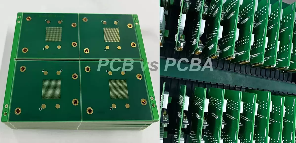
Fixed pattern noise is the variation between pixels or between readout channels that does not change with the scene. Some of it is inherent to the sensor, but a significant part is contributed by the board: differences in trace length to different channels, differences in the reference seen by different amplifiers, and thermal gradients that make one end of the array behave differently from the other.
Designing for calibration means making those differences small and stable rather than eliminating them entirely. Symmetric layout, matched trace lengths and a shared reference for all channels mean the residual error is a simple function that a calibration can remove. Where the error changes with temperature, the calibration has to be repeated at the operating temperature, or the design has to keep the temperature stable.
Testing and Validation
An imaging board is validated with a known target rather than a signal generator. A uniform illumination test measures the fixed pattern noise directly, a dark frame measures the offset and the dark current, and a resolution target measures the modulation transfer function. Those measurements are repeated at the temperature extremes, because the failure mode that matters is an image that is acceptable in the laboratory and degraded in service.
Electrical measurement still has its place. Power supply noise is measured at the sensor pins rather than at the regulator, jitter is measured at the sampling clock, and the readout channels are checked for gain and offset matching. Our design release checklist places those measurements in the review sequence before a layout is released for production.
Choosing Between Sensor Technologies
The choice of image sensor shapes the rest of the board. A charge coupled device requires a multi-phase clock, a bias network with several precisely sequenced rails and an analogue front end with correlated double sampling, so the board carries a significant amount of analogue circuitry that it must keep quiet. A complementary metal oxide image sensor performs much of that work internally, so the board supplies a smaller number of rails but must still provide a clean clock and a low jitter sampling signal, and the interface becomes a high speed digital link that must be treated as a transmission line.
The practical consequence is that the same optical performance can lead to very different boards. Where the sensor has the conversion inside it, the design effort moves from analogue quietness to digital signal integrity and power distribution. Where the conversion is external, the reverse is true. Deciding that early, rather than after the layout has started, is what keeps the noise budget achievable.
FAQ
Why not use a switching supply for the analogue rails? Because its output ripple appears in the image as a pattern related to the switching frequency. A linear regulator after the switcher, placed close to the load, is the usual compromise.
Does trace length matching matter on an imaging board? It matters wherever several channels are read in parallel, because a length difference produces a timing difference that appears as a channel to channel variation in the image.
What is the most common cause of banding in an image? Coupling from a switching supply or a digital clock into the analogue reference, which produces a repeating pattern tied to the interfering frequency rather than to the scene.