Fingerprint Sensor FPC: Design and Assembly Considerations
A fingerprint sensor FPC is one of the tightest flexible interconnects in a consumer product, and a fingerprint sensor sits under glass, behind a button or on the back of a phone, and the flexible circuit that connects it carries a dense array of fine traces through a very tight space. It is one of the most demanding flexible designs in consumer electronics.
Why the Sensor Uses a Flexible Circuit
The sensing element is typically a small die or an array of electrodes that must be positioned precisely relative to the glass, while the processing electronics sit somewhere more convenient. A rigid board cannot make that connection without a connector and a cable in a space that has room for neither.
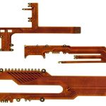
A flexible circuit solves both problems. It can be bonded directly to the sensor, routed around the components behind the display and terminated at a board-to-board connector, and it does all of this at a thickness measured in tens of microns.
Substrate and Thickness Requirements
The polyimide substrate is chosen for thinness and dimensional stability rather than for electrical performance. A thin, adhesiveless construction keeps the total stack low, which matters when the assembly must fit between the glass and the chassis without creating a visible bump.
Thickness uniformity matters as much as the average value. A variation across the sensing area changes the distance between the electrodes and the finger, which affects the measured capacitance and therefore the image quality.
Fine Line Traces and Array Routing
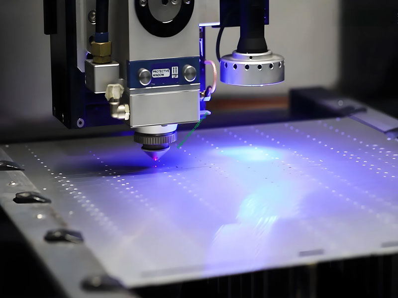
The sensor array itself may contain hundreds of channels, each of which has to reach the edge of the circuit and then travel to the connector. That concentration of traces forces the finest lines the process can produce, with narrow spacing and minimal clearance.
Resistance becomes a factor at these widths. A long fine trace has enough resistance to slow the charge transfer used by capacitive sensing, so the design balances trace width against the available routing space rather than using the minimum everywhere.
Shielding and Noise Immunity
Capacitive sensing measures a very small change in capacitance, which makes the routing vulnerable to interference. A ground plane or a guard structure alongside the sensing traces reduces coupling from the display, the radio and the power circuits that share the same small volume.
Shielding has to be designed with the sensing in mind. A solid ground plane directly under the electrodes adds parasitic capacitance to every channel and reduces the sensitivity of the measurement, so the shielding is normally placed beside or around the sensing area rather than beneath it.
Bonding to the Sensor and the Glass
The circuit is usually bonded to the sensor die or the electrode pattern with an anisotropic conductive film or an adhesive, and the bond has to survive the assembly process and the life of the product while maintaining alignment within a few tens of microns.
Thermal expansion is the enemy here. The flexible circuit, the adhesive and the glass all expand by different amounts, so the bonding process is designed to minimise the temperature excursion and the finished assembly is tested across the operating range for alignment drift.
Bend Limits and Mechanical Design
Fingerprint modules involve several bends, including a fold to route the circuit into the chassis and an S-bend to accommodate assembly tolerance. Each bend has a minimum radius, and the traces must cross the bend line perpendicularly.
Dynamic bending is avoided entirely in most designs; the circuit is bent once during assembly and then remains static. Where the assembly involves movement, such as a sensor behind a moving part, the design must be qualified with a flex test at the specified radius.
Assembly Tolerance and Handling
The circuit is thin, small and easily damaged. Handling requires a carrier or a frame until the sensor is attached, and the assembly process is designed so that the flexible part is supported at every stage.
Alignment tolerance is the critical parameter. The difference between the sensor position and the glass aperture determines how much of the finger makes contact with the sensing area, and a small misalignment shows up as a reduced acceptance rate rather than as a hard failure. Designing the tolerance stack deliberately, rather than assuming the process will hold it, is what keeps a fingerprint module working in production.
Testing and Qualification
Testing covers both electrical continuity and optical or capacitive performance. A continuity test confirms the routing, while a measurement of capacitance per channel, or an image captured through the glass, confirms that the assembly performs as intended.
Because the failure modes are often mechanical, qualification includes thermal cycling, humidity exposure and a drop test on the finished product. Alignment after cycling is measured directly, since a shift of a few tens of microns can degrade the sensor enough to fail a customer acceptance criterion. Where the design also uses a thin flexible structure, the handling constraints described in the discussion of ultra-thin flexible circuits apply directly.
Comparing Flexible and Rigid Approaches
A rigid board with a separate sensor module is cheaper to produce and easier to test, and it remains the choice where there is room for it. The flexible circuit wins when the mechanical envelope leaves no alternative, which is the usual situation in a modern handset.
Where the design sits between the two, a rigid-flex construction can carry the sensing area on a rigid section and route the connection on the flexible tail. That option reduces assembly steps and removes a connector pair, at the cost of a more complex fabrication process, as discussed in flexible interconnect selection.
What a Fingerprint Sensor FPC Has to Deliver
The part carries a sensor array, a small amount of local processing and a connector, all on a strip of polyimide thin enough to bend behind a display. A fingerprint sensor FPC therefore has to hold fine line traces at tight pitch over a short run, keep the impedance and the stray capacitance stable while the tail is flexed during assembly, and survive the heat of the bonding process without losing registration between the sensor pads and the trace ends.
Those three requirements pull against each other. Thinner copper helps the fine line etch but raises resistance; a thicker coverlay protects the traces but stiffens the bend region; a larger pad helps the bonder but wastes the space the array needs. The design that works is the one where the bend radius, the trace width and the bonding pad geometry were chosen together rather than in sequence, and where the stackup was fixed before the layout was drawn.
Documenting the bend zone in the fabrication drawing matters as much as the layout itself. The flex direction, the minimum radius and the number of expected flex cycles should appear on the drawing, because the coverlay opening and the stiffener placement depend on them. Where the tail bends close to the connector, a stiffener on the connector end is normal practice, as outlined in flex and rigid-flex construction.
FAQ
Can a fingerprint sensor circuit be made on a standard flexible process? The routing is within what a fine-line flexible process can hold, but the thickness uniformity and the alignment tolerance are tighter than a general purpose interconnect requires. The process has to be specified rather than assumed.
Why is a ground plane under the electrodes avoided? Because it adds parasitic capacitance in parallel with the finger, reducing the relative change the sensor measures. Shielding beside the traces achieves most of the noise immunity without that penalty.
How thick is the flexible circuit in a typical module? Constructions in the range of 50 to 100 microns total are common, with thinner variants used where the assembly height is critical. The limit is usually set by the handling and bonding process rather than by the material.