Satellite Communication PCB: Manufacturing and Design Guide
A satellite communication terminal is a radio that must work once, in a place where it cannot be repaired, after a launch that subjects it to levels of vibration and acoustic energy that no terrestrial product sees. The board inside it is designed for that single set of conditions, and the consequences are visible in every choice: materials that do not outgas in vacuum, joints that survive thermal cycling between light and shadow, and an electrical design that has no single point of failure.
What the Board Has to Deliver
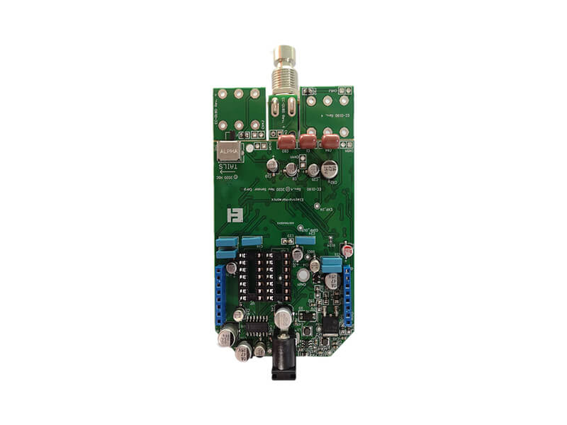
A satellite communication board carries a radio frequency chain, a digital modem, a power converter and the interface to the spacecraft bus. The radio frequency section handles signals at power levels spanning many orders of magnitude, from a transmit amplifier delivering watts to a receiver resolving a signal far below the noise floor of a terrestrial system. Isolation between those two is achieved by physical separation, by shielding and by the stack-up rather than by filtering alone.
The digital section performs modulation, coding and error correction, and it is frequently implemented in a programmable device so that the waveform can be updated in orbit. That flexibility is worth a great deal, because a spacecraft cannot be recalled, but it also means the device is the largest and most demanding component on the board.
Materials and Vacuum Behaviour
Thermal vacuum is the defining environment. There is no air to conduct heat and no air to suppress it, so the board must be able to transfer heat by conduction into a structural path and must tolerate large temperature swings as it moves between sunlight and shadow. Materials are selected for low outgassing, because anything that evaporates in vacuum can condense on optical surfaces, on thermal radiators or on the very radio frequency hardware it was meant to protect. That includes the laminate, the solder mask, the conformal coating and every adhesive used in the assembly.
Polyimide laminates are common because they tolerate the temperature range and can be made thin without losing mechanical integrity, though they absorb more moisture than FR-4 and require a bake before assembly. A symmetric stack-up is mandatory rather than preferred, because an unbalanced construction will bow and every joint on a bowed board carries stress. Our component tolerance and reliability notes describe how those stresses are estimated.
Thermal Cycling and Joint Fatigue
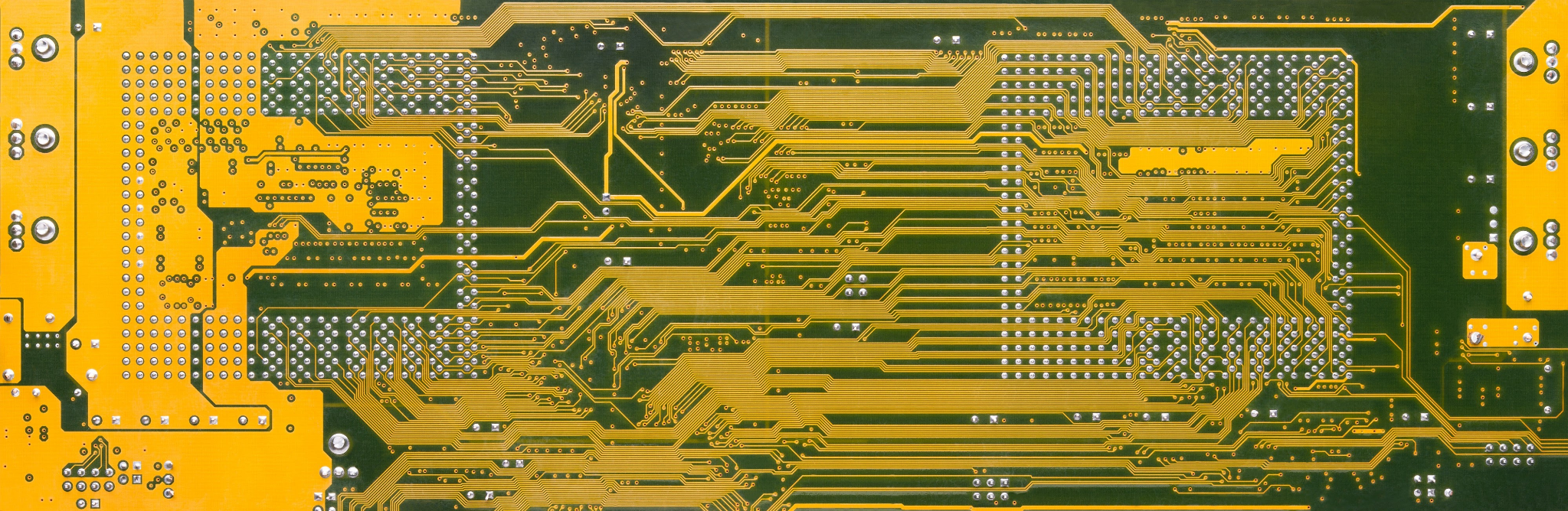
The temperature swings in orbit are large and frequent. Each cycle consumes part of the fatigue life of every plated through hole and every solder joint, and the weakest points are the ones where a rigid element meets a compliant one. A plated barrel in a thick board, a large component with stiff leads and a ceramic package on a flexing laminate are all candidates for a crack that opens after a few thousand cycles.
Design measures reduce the strain rather than eliminating it. Thinner boards flex more easily and concentrate less strain. High aspect ratio holes should be avoided because a small hole in a thick board concentrates it further. Where a large component must be used, a compliant mounting or a mechanical restraint takes the load away from the solder joint, and underfill distributes the strain across a ball grid array rather than leaving it at the corners. Our thermal management article describes how the thermal path is arranged.
Radio Frequency Discipline
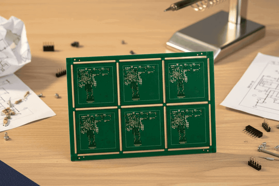
The radio frequency chain is laid out as a transmission line from the modulator to the antenna port, with controlled impedance, a continuous reference plane and ground vias at every transition. At the frequencies used for satellite links, a discontinuity of a few tenths of a millimetre is enough to produce a reflection that degrades the link margin, so the layout is verified by measurement rather than by inspection.
Isolation between the transmit and receive paths is a layout property before it is a filter specification. Separate the two as far as the board allows, put grounded copper between them, and use shielded enclosures over the sensitive sections. The transmit amplifier also needs its own thermal path, because the efficiency of a radio frequency amplifier is modest and the rejected power becomes heat in a package with almost no surface area.
Redundancy and Fault Tolerance
A spacecraft has no maintenance, so the design assumes that a component will fail and arranges for the system to survive it. That usually means redundant signal paths, with the switching arranged so that a single failed component cannot disable both, and it means the redundancy extends to the board layout: two paths that share a via, a plane or a connector pin are not redundant in any useful sense.
The power system follows the same logic. Multiple rails, current limiting on each, and a protection arrangement that isolates a faulted load rather than shutting down the whole board are standard. Where a single event can latch a device, a watchdog or a supply cycling circuit is provided, and it is designed to operate without ground intervention.
Qualification Testing
Every part of the design is proved by test. Vibration and acoustic testing subjects the assembled board to the launch profile, thermal vacuum testing cycles it between the temperature extremes in a vacuum chamber, and electrical performance is measured before and after each of those. The failures that matter are the intermittent ones, so the measurements are made during the test rather than only at the end.
Radiation testing is often required as well. Total dose affects the long term behaviour of the semiconductors, and single event effects can cause a transient fault or a latch-up. Parts are selected for their radiation tolerance, and the design includes mitigation for the effects that cannot be avoided. Our design release checklist places those checks in the sequence that catches cheap problems before the expensive campaign begins.
Manufacturing for a Single Build
A satellite programme usually builds a very small number of flight units, which changes the relationship between the design and the fabricator. There is no opportunity to learn from a production run, so the process is qualified in advance: coupons are built and tested, microsections are taken from a representative panel, and the plating thickness and registration are confirmed before the flight hardware is started. The documentation that accompanies the board is part of the deliverable, because a board that cannot be traced to its material lot cannot be cleared for flight.
Assembly follows the same logic. Each board is inspected under magnification, x-rayed where joints are hidden, and electrically tested on every net. Conformal coating is applied and cured under controlled conditions, and the finished assembly is photographed for the record. The cost of that process is high in absolute terms, but it is a small fraction of the programme, which is why the discipline is maintained even when the schedule is tight.
FAQ
Why is outgassing such a concern in a vacuum? Because anything that evaporates has nowhere to go. It condenses on the coldest surface it can reach, which may be an optical element, a radiator or a radio frequency component, and it can disable the mission.
What is the most common failure mechanism on a satellite board? Thermal cycling fatigue at plated through holes and solder joints, followed by radiation induced effects in the semiconductors.
Can a satellite board be repaired? No, which is why redundancy is designed into the layout rather than added as a spare component. A redundant path that shares a connector pin is not redundant at all.