Semiflex PCB: Rigid Boards With a Controlled Bend Region
A Semiflex PCB is a rigid FR-4 board that has been locally thinned so that it can be bent once during assembly. It uses the same materials and the same fabrication sequence as an ordinary multilayer board, which is what makes it inexpensive compared with a flex or rigid-flex construction.
The bend is permanent and normally performed once, by hand or with a fixture, after assembly. The technology exists to replace a connector and a cable with a continuous board, which removes a connection, saves volume and improves reliability at modest cost.
What Makes a Board Semiflex
The distinguishing feature is partial thinning. In the bend region, the laminate is milled down so that only a thin layer of FR-4 remains, leaving the copper conductors intact on one or both sides.
The rest of the board is conventional multilayer FR-4, so components, vias and impedance-controlled routes are designed with standard rules outside the bend area.
The result is a board that is rigid where it must be and compliant in one defined zone. It is not a flexible circuit and must not be treated as one: repeated bending in the thinned region will crack the copper.
How Partial Thinning Is Produced
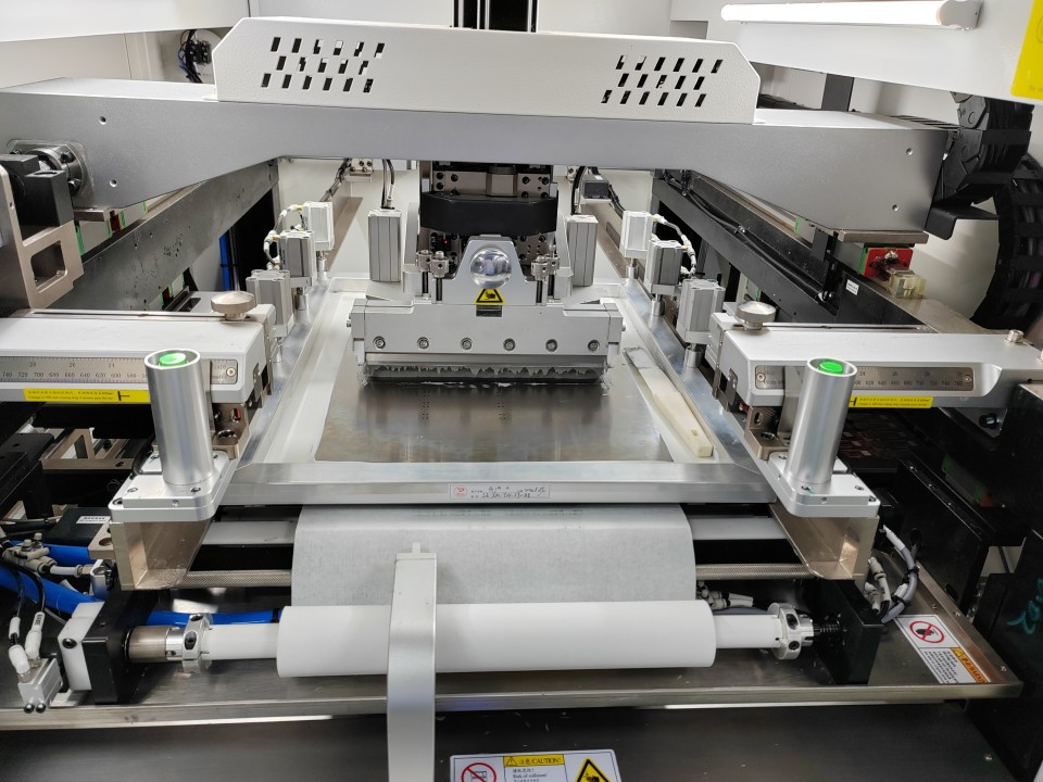
Thinning is performed by controlled-depth milling after the board is laminated. The milling depth must remove the resin and glass without cutting the remaining copper, so the process requires precise depth control and careful tooling.
Some designs thin from both sides to remove more material while keeping the conductors embedded symmetrically, which improves bend performance because the neutral axis stays near the conductors.
The milling operation leaves a surface that is not solder mask quality. In most designs the bend region is left masked only lightly or not at all, and the drawing must state what is permitted.

Bend Radius and One-Time Bending
The achievable bend radius depends on the remaining thickness and on the number of copper layers left in the bend region. A thinner remaining stack allows a tighter bend, but the copper becomes more vulnerable to cracking.
The bend should be specified as a radius rather than an angle, because the strain in the copper depends on the radius of curvature. A bend formed over a sharp corner produces local strain far above the average and cracks the conductor there.
One-time bending is the design assumption. Where a product needs repeated movement, a flexible or rigid-flex construction is required, and the semiflex approach will fail at the first few cycles.
Design Rules for the Bend Region
Keep the bend region free of vias, plated holes and components. A plated barrel cannot bend, and a via in the thinned area is a guaranteed crack.
Route conductors across the bend perpendicular to the bend line rather than parallel to it, and keep them as wide as the routing allows. Where several conductors cross the bend, keep them evenly spaced so the strain is distributed.
Extend the thinned region beyond the actual bend on both sides. Stress concentrates at the boundary of a stiffness change, so the transition should be gradual rather than abrupt.
Materials and Layer Structure
Standard FR-4 is used throughout, which is what makes the construction inexpensive. The remaining thickness in the bend region is typically 0.2 to 0.4 millimetres depending on the total stack.
Symmetry matters. A stack that is unbalanced will curl when thinned, and the curl makes the board difficult to position in the assembly fixture. Copper balance across the thinned region reduces that tendency.
Where the remaining dielectric must be thinner than a single laminate ply, the design is usually restructured so that the bend occurs in a prepreg-free region, because a single ply cannot be thinned further without cutting through it.
Bend Area and the Assembly Fixture
The bend is usually formed after reflow, because a bent board will not sit flat for printing and placement. The assembly fixture therefore holds the board flat and the bend is performed as a separate operation.
The fixture defines the radius and the position of the bend, so it is a quality control tool as much as an assembly aid. A bend performed without a fixture gives a radius that varies from unit to unit, and the variation is what causes field failures.
Where Semiflex Is the Right Choice
It fits products that need to fold a board once to fit a smaller enclosure, that want to replace a board-to-board connector and cable, or that need a rigid board with one articulated section.
Typical examples include camera modules, sensor heads, small instruments and handheld devices where a rigid horizontal board and a vertical display board must be joined reliably.
It does not fit products that flex repeatedly, that must be bent to a very tight radius, or that need dynamic movement. Those requirements belong to flex or rigid-flex designs.
Reliability and Failure Modes
Failures in a semiflex board are concentrated in the thinned region. The most common is a cracked conductor at the edge of the thinned area, where the stiffness changes abruptly and the strain is highest.
The second is delamination between the remaining laminate and the copper, caused by moisture absorbed during processing and released during the bend or during reflow. Baking before assembly and keeping the thinned area clean reduce that risk.
The third is mechanical damage during handling, because the thinned region is fragile before it is formed. Carriers and handling rules for the assembly line are part of the design approval rather than an operational detail.
Verification and Acceptance
Verification is straightforward and should be performed on the first build. The board is bent to the specified radius in the fixture, and continuity is measured across the conductors that cross the bend.
Microsectioning a sample at the bend boundary shows whether the copper has cracked or whether the laminate has separated. That single check explains most of the failures that would otherwise appear as intermittent opens in the field.
Cost Compared With Alternatives
The fabrication cost is close to a standard multilayer board plus the milling operation, which makes it considerably cheaper than a rigid-flex stack that requires polyimide, coverlay and additional lamination steps.
Assembly cost is lower than a connector-plus-cable arrangement, because there is no separate cable to fit, no connector to mate and no second board to align. Reliability improves for the same reason: the connection is copper rather than a contact pair.
The trade is design constraint. The bend region must remain free of components and vias, which consumes board area, and the bend must be a single event performed with a controlled fixture.
Design Checklist
Confirm that the bend is performed once, define the bend radius rather than the angle, keep the bend region free of vias and components, and specify the thinned thickness and the permitted surface condition on the drawing.
Then define the assembly sequence and the fixture. Where the board is bent before assembly, the placement process must handle a non-flat panel, which is usually a more expensive and less reliable approach.
Related reading: multilayer prototype requirements, board outline and mounting design, and PCBA development process.
FAQ
Can a Semiflex board be bent more than once? It is designed for a single forming operation. Repeated bending in the thinned region fatigues the copper and eventually causes an open circuit.
How tight a radius is possible? It depends on the remaining thickness and the number of copper layers in the bend region. The supplier should confirm the achievable radius for the specific stack before the layout is finalized.
Is Semiflex cheaper than rigid-flex? Yes, substantially, because it uses standard FR-4 and the same fabrication flow as a conventional multilayer board, with only a milling operation added.