Spectrum Analyzer PCB Layout: Shielding, Phase Noise and Spurs
A spectrum analyzer is an instrument that measures a signal it is not allowed to disturb. The board therefore carries a receiver with a very wide dynamic range, a synthesizer whose phase noise sets the resolution limit, and enough isolation between its own blocks that the display never shows an artefact the instrument created itself.
Those requirements make the spectrum analyzer PCB a study in partitioning. The sections below cover the receive chain, the shielding strategy, synthesizer layout, grounding of the sensitive analog blocks and the calibration access that production test needs.
The Receive Chain in Blocks
The signal path normally starts with an attenuator and a preselector, continues through one or two mixer stages, and ends in a narrowband intermediate-frequency filter followed by a logarithmic detector or a digital converter. Each block has a different impedance environment, and the transitions between them are where most of the stray response in a first prototype comes from.
An image-reject or double-conversion architecture is common because it pushes the image frequency far from the band of interest. The price is a second local oscillator and another filter, and the layout has to keep the two oscillator signals isolated from each other and from the intermediate-frequency chain.
Shielding and Isolation
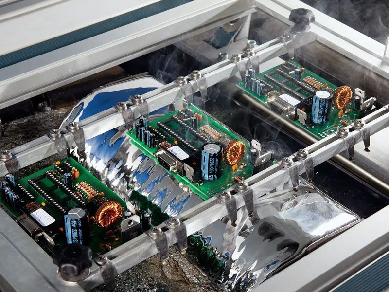
Isolation is achieved with copper, not with software. A fence of ground vias along both sides of a microstrip line, a cast shield can with a soldered or gasketed perimeter, and separate cavities for the synthesizer and the detector are the usual measures on a spectrum analyzer PCB.
The shield can is only as effective as its grounding. Vias are placed at intervals well below a quarter wavelength at the highest internal frequency, so that the cavity walls behave as continuous metal rather than as a resonant slot, and the lid contacts are kept close to the wall vias.
Synthesizer and Reference Layout
Phase noise is decided long before the signal reaches the front end. The reference oscillator, its buffer and the phase detector loop filter are laid out as a compact block with a local ground plane, and the loop filter components sit against the charge pump pins so that no digital return current flows through that copper.
The reference is usually kept on the same board as the synthesizer rather than distributed across a cable, because a cable adds both loss and pickup. Where the reference has to be shared, it is distributed as a differential pair or through a dedicated buffer with its own supply filtering.
Grounding and Power for Sensitive Analog Blocks
A single ground plane with careful partitioning is easier to control than a split plane, provided the partition is respected by the layout. Analog return currents are kept on the analog side of the board, the digital section keeps its own local loop, and the two meet at one defined point beneath the data converter.
Supply filtering follows the same principle. Each amplifier and mixer receives its own series ferrite or resistor with local decoupling, and the low-noise blocks nearest the input are fed from a regulator that does not also supply the digital section. On a spectrum analyzer PCB the difference between a clean supply and a shared one is visible as spurious lines on the display.
Calibration Access and Test
Production calibration needs injection points, and they have to be designed in. A switched calibration path at the input, a test pad on the intermediate-frequency chain and a way to measure the reference frequency without opening the shield all shorten the test time considerably.
The board also benefits from a defined power-up sequence, because a mixer that is enabled before its local oscillator is present will convert whatever is on its ports and produce a transient that test equipment may interpret as a failure.
Thermal and Mechanical Considerations
An instrument that runs continuously generates a steady heat load, and the frequency response of a narrowband filter drifts with temperature. Placing the filters and the reference away from the regulators, and giving the power section its own copper area with thermal vias to the chassis, keeps the drift inside the calibration budget.
Mechanically, the shield cans, the connectors and the board outline have to be defined together. A connector that moves when a cable is tightened will change the response of the circuit behind it, and no amount of shielding compensates for a board that flexes in the housing.
Digital Control and Display Interface
The instrument is a mixed signal system, and the digital section sits on the same board as the receiver. A touch controller, a display link and a processor bus all switch at tens or hundreds of megahertz, and every one of them is a potential source of small signals at the frequencies the receiver is trying to measure.
The usual answer is distance plus a disciplined return path. Digital traces are grouped over their own ground plane and kept off the front end side of the board, and any trace that has to cross the boundary does so over an unbroken reference with a ground via placed beside the transition. Where the processor connects into the shield covered analog area, the interface is filtered at the boundary rather than at the source.
Design Review Checklist
Before the layout is released, check the isolation plan against the block diagram: which cavities exist, what feeds each of them, and where every cable and connector enters the shielded area. Then check the analog supply tree, the local oscillator paths and the image rejection filtering, because those three items decide whether the instrument meets its published specification.
Finally, review the test access. A spectrum analyzer PCB that cannot be calibrated without removing a shield can will spend more time on the test bench than in production, and every minute of calibration is a cost that the design can remove in advance by adding a switched injection path and a few test pads in the right places.
Related reading: high-frequency trace routing, microstrip and stripline routing, power plane splitting rules, and ground current and harmonic distortion.
Front-End Protection and Attenuator Design
The input of a spectrum analyzer is the most exposed node in the instrument. A user will connect a transmitter, forget the attenuator setting, and expect the instrument to survive. The protection network therefore sits ahead of the first amplifier: a fused or switched attenuator, a DC block, and a pair of anti-parallel diodes that clamp an overload before it reaches the active devices.
Those parts add capacitance and a small series resistance, so they are placed on a short, wide trace with the ground return directly beneath, and the parasitic capacitance is accounted for in the calibration table rather than left as an unknown. Where the attenuator is switched, the relay or solid-state switch is positioned so that all of its unused positions are terminated, because an open port on a switch is an antenna inside the shield can.
Mechanical Integration and Assembly
The shield cans, the connectors and the chassis form one mechanical system. The board outline is designed so that each shield footprint lands on a flat area supported by the enclosure, and the connectors are anchored to the chassis rather than held only by their solder joints, because a connector that moves under cable torque changes the response of the circuit behind it.
Where a spectrum analyzer PCB has a castellated or edge-launched RF port, the launch geometry is defined together with the housing so that the transition into the internal transmission line is repeatable from unit to unit. gopcb builds instrument boards with controlled impedance, selective shielding footprints and panel level processes that keep the RF launch geometry consistent across a production batch.

FAQ
Why does a spectrum analyzer PCB need so much shielding? Because the instrument measures small signals in the presence of its own oscillators and digital clocks. Without shielding and via fencing, those signals couple into the front end and appear as false responses.
What sets the resolution bandwidth floor? The phase noise of the first local oscillator and the selectivity of the intermediate-frequency filters. Both are layout sensitive, so the synthesizer deserves its own quiet ground and supply.
Is a split ground plane necessary? Usually not. A single plane with disciplined partitioning and one defined meeting point between analog and digital returns is easier to control than a split, and it avoids routing discontinuities.