Ultrasound PCB Design: Beamforming Front Ends and Medical Assembly
An ultrasound board is an analog instrument built around a large number of nearly identical channels. A probe array presents 64, 128 or 192 elements, and each element needs its own transmit driver, its own receive path and its own delay, all matched closely enough that the beam formed in software behaves as if it had been formed in hardware.
That requirement shapes every part of the ultrasound PCB: the stackup, the layer assignment, the grounding scheme, the probe connector and even the choice of solder mask. The sections below walk through the decisions behind a medical ultrasound board, from the low-noise receive chain to the assembly rules that a regulated product has to satisfy.
Noise Floor and Dynamic Range
The receive chain begins with a low-noise amplifier placed as close to the connector as the mechanical layout allows, because every centimetre of trace before the first stage adds capacitance and picks up interference that no later gain can remove. The noise figure of that stage sets the smallest echo the system can detect, while the channel dynamic range sets the largest.
A typical channel has to resolve echoes spanning roughly 60 to 80 dB, so the front end is built as a low-noise amplifier followed by a time-gain-compensation stage whose gain ramps up as the echo returns from deeper tissue. The ramp is generated in the analog domain, and its accuracy directly affects the brightness uniformity of the image.
Channel-to-Channel Matching
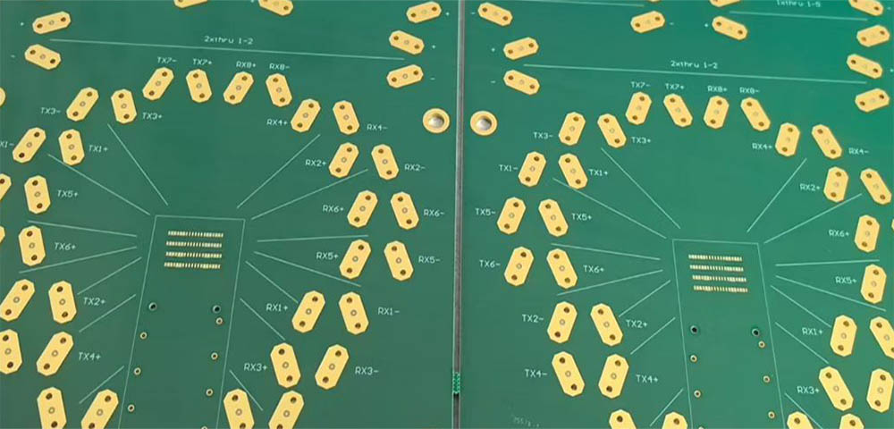
Delay accuracy is what turns a set of channels into a beam. An error of 10 ns between two elements steers the focus away from the intended point, so the routing is length matched, usually to within a few mils across the whole array, and the components in each channel are taken from the same tolerance band.
Where the delay is implemented digitally, the matching problem moves into the clock distribution: the sampling clocks for every channel must arrive with the same skew, which usually means a balanced clock tree and a dedicated reference plane rather than a shared digital supply.
Stackup and Material Selection
An ultrasound PCB is normally an eight to twelve layer board. A single FR-4 grade is often adequate for the receive band, because the operating frequencies are low compared with microwave hardware, but the transmit and switching sections benefit from a low-loss laminate and from copper weights that keep the pulse edges clean.
Layer assignment matters more than the material choice. Each analog channel gets a signal layer referenced to a solid ground plane, the high-voltage transmit section gets its own quiet pair of layers, and the digital processing is kept on separate planes so that its return currents never share copper with the receive path.
Transmit Path and High-Voltage Rules
Transmit drivers deliver pulses of 100 V or more, and the layout has to respect creepage and clearance distances that a low-voltage board never considers. Slots milled through the board, routed isolation barriers and wide spacing around the high-voltage nodes are all standard practice on this class of hardware.
The discharge path deserves the same attention as the drive path. Bleeder resistors, a defined discharge time and a physical layout that keeps the stored energy away from the probe connector all reduce the risk that a fault reaches the patient interface.
Probe Interface and Cable Termination
The probe cable carries one coaxial conductor per element, and terminating 128 micro-coaxial lines into a board a few centimetres wide is a mechanical problem as much as an electrical one. The connector footprint, the strain relief and the bonding method are chosen together, and the transition from cable to trace is kept short.
Where an anisotropic conductive film is used, the bond pitch and the pad finish have to be compatible with the film, and the assembly is inspected by measuring contact resistance per element rather than by sampling. A shorted or open element is visible in the image, but only after the whole probe is built.
Assembly, Coating and Hygiene
Medical assembly brings requirements that change the fabrication plan: documented traceability, controlled cleaning, and a coating decision made early because it affects rework. On an ultrasound PCB the conformal coating protects the high-impedance receive nodes from humidity and from the cleaning agents used between examinations.
Residue from the soldering process is a design issue as well, because ionic contamination under a high-impedance node produces leakage that drifts with ambient moisture. Where the board has to be water washed, the components and the finish are selected accordingly, and the cleaning is verified rather than assumed.

Verification and Production Data
Production test on a medical ultrasound board is per channel: gain, phase, noise floor, crosstalk and pulse shape are recorded for every element, and the results are kept with the serial number of the assembly. A board that passes on average but fails on two channels is not a passing board.
Producing an ultrasound PCB also means holding tighter fabrication tolerances than a consumer product, since layer-to-layer registration and impedance control translate directly into channel matching. gopcb builds these boards with controlled impedance and per-channel electrical test data so that the imaging software receives a front end it can calibrate predictably.
Digital Back End and Data Path
The digitised channel data leaves the analog section at a rate that would embarrass a consumer board. A 128 channel system sampling at 40 to 65 MSa/s produces several gigabits per second before any beamforming takes place, and all of that traffic has to cross the board without disturbing the receive path it sits beside.
Serialiser lanes are routed as controlled impedance differential pairs with their own reference plane, kept well away from the analog traces, and terminated at the destination rather than in the middle of the board. Where the beamformer sits on a separate card, the interface between the two boards is defined as a connector with a matched pinout so that the pair lengths stay balanced through the transition.
Design Review Checklist
Before release, confirm that every receive channel has the same number of vias, that the transmit and receive sections share no copper pour, that the high-voltage isolation barriers meet the creepage distances required by the applicable medical standard, and that the probe connector footprint has been verified against a physical sample rather than against a drawing.
Then check the supply tree: which blocks share a regulator, where the return currents flow, and whether any digital clock crosses a plane boundary. On an ultrasound PCB these three questions explain the majority of the faults that survive first article inspection, and all of them are cheaper to answer on a schematic than on a finished board.
Related reading: mixed-signal PCB design guidelines, conformal coating and board protection, and PCB manufacturing tolerances.
FAQ
Why does an ultrasound PCB need so many layers? Because every receive channel needs an undisturbed reference plane and its own routing space. Once the analog channels, the high-voltage transmit section and the digital processing are separated, eight to twelve layers is the practical minimum.
What limits channel-to-channel matching? Trace length, dielectric variation, connector parasitics and component tolerance, in roughly that order. The layout controls the first two, so matching is designed in rather than corrected in firmware.
Can a standard FR-4 laminate be used? For the receive band, usually yes. The transmit drivers and any high-speed digital interfaces benefit from a low-loss material and from copper weights that keep switching losses under control.