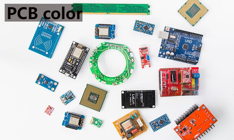
Module Board Design: Partitioning, Interfaces and Shielding
A module board is a small circuit that performs one function and connects to the rest of the system through a defined interface. Power modules, display drivers, radio transceivers, sensor front ends and motor controllers are all built this way. The approach reduces design effort and simplifies certification, but it moves complexity into the interface, the mechanical stack and the test strategy.
What Counts as a Module Board
The defining feature is a boundary. A module has inputs, outputs, a supply and a mechanical outline, and everything inside that boundary is the module designer’s responsibility. Whether it is a separate board with its own connector or a shielded block on a larger board, the boundary is what makes the design reusable.
Reuse is the main benefit. Once a power module is qualified, it can be used in several products without repeating the design work, and a pre-certified radio module can remove an entire radio approval exercise from the programme.
Partitioning the System
Partitioning is the first design decision and the hardest to reverse. Group functions that change together, and separate those that have different noise, thermal or regulatory characteristics. A sensitive analogue front end should not share a module with a switching power stage, even if both are small enough to fit.
Count the interfaces that the partition creates. Every boundary adds connectors, cables and a place for a signal to degrade. A partition that produces twenty signals across a connector may cost more in connectors and board area than keeping the function on one board, so the split has to be justified by reuse, certification or mechanical necessity. Related layout decisions are discussed in the notes on PCB design quality characteristics.
Defining the Interface
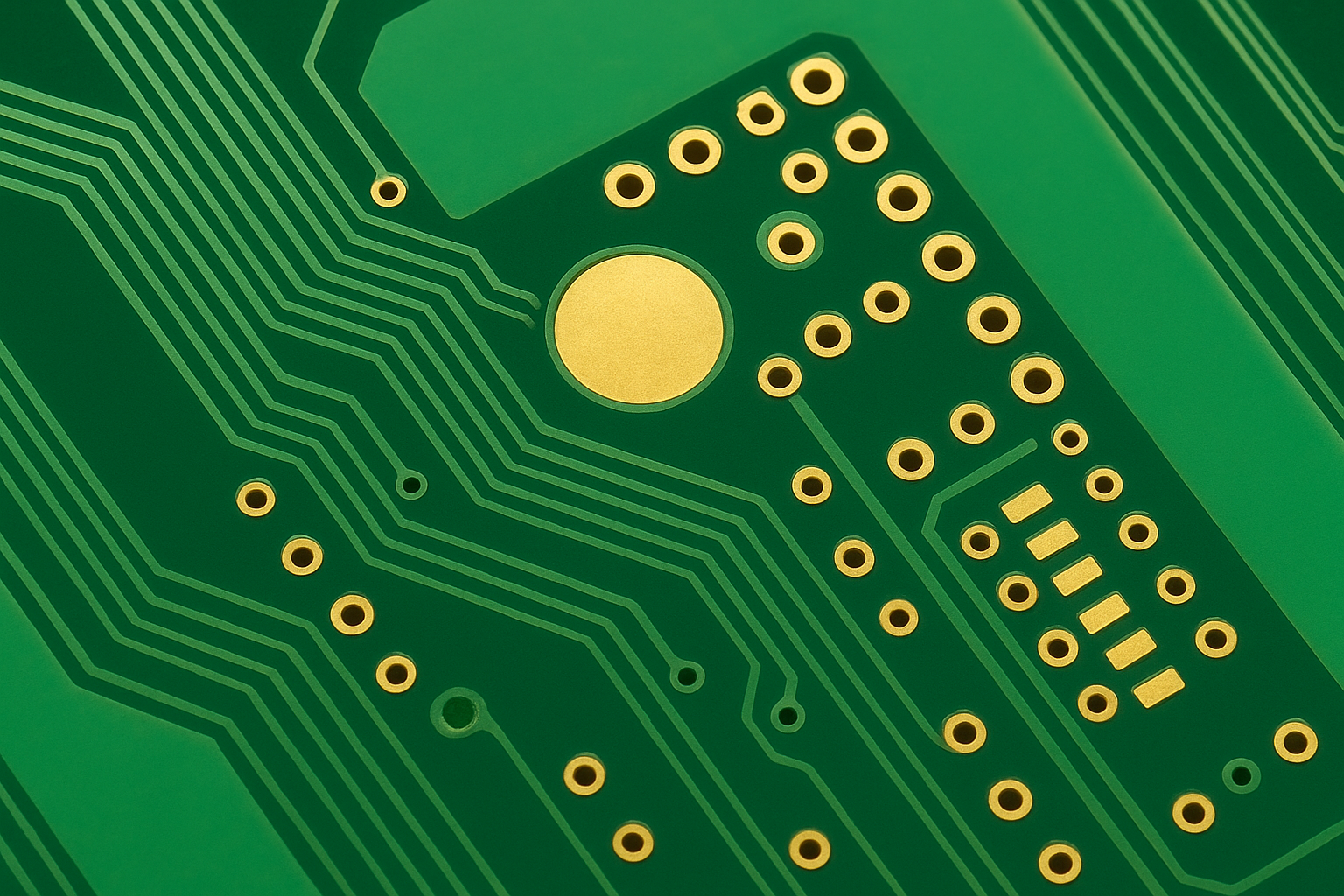
Write the interface down as a specification before either side is designed. Pin assignment, signal levels, impedance, timing, supply current, power sequencing and the connector part number all belong in it, along with the mechanical envelope and the tolerance on the mating position.
Assign ground pins generously and interleave them with high speed signals. A connector that carries a fast interface with only one or two ground pins will radiate and will be sensitive to noise, no matter how good the layout on either board is. Where the interface carries differential pairs, the connector should be chosen so that each pair has an adjacent ground.
Board-to-Board Connectors and Stacking
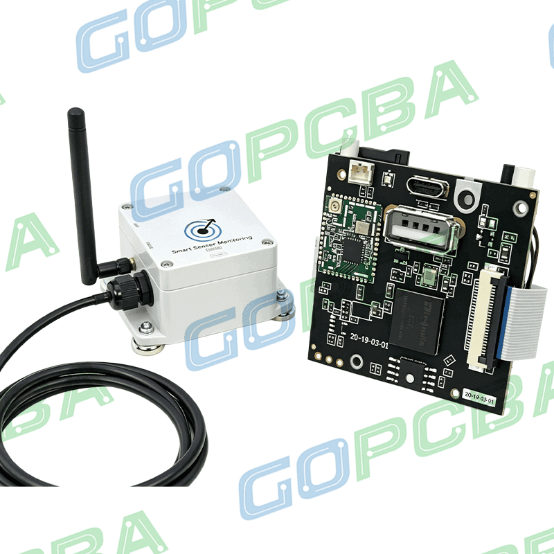
A board-to-board connector fixes both the electrical interface and the mechanical relationship between the two boards. Height, pitch, current rating and the number of mating cycles are the parameters that matter, together with the alignment tolerance the connector can absorb.
Stacking two boards introduces a mechanical problem: the boards must be held in alignment, and the connector pins should not carry the mechanical load. Stand offs or mounting pillars are used to support the assembly, and the connector is positioned so that insertion force is not transmitted through the solder joints. A high pin count board-to-board connector needs support at both ends as well as in the middle, because the insertion force accumulates along the row and can bow the board if only the ends are fixed. Where the stack has to survive vibration, the mechanical fastening rather than the connector is what keeps it together.
Shielding and Radio Modules
A module that contains a radio or a fast clock usually needs shielding. A pressed metal can soldered to a ground ring around the circuit confines emissions and protects the receiver from outside interference. The can adds height and cost and complicates rework, so it should be justified by a measurement rather than by habit.
Antenna keep-out is equally important. The area around an antenna must be free of copper, and in a stacked assembly the other board can detune the antenna if it comes too close. The mechanical stack and the antenna position therefore have to be designed together, and the enclosure material matters as well.
Test Access at Module Level
A module that cannot be tested on its own forces the whole assembly to be debugged as a unit, which is slow and expensive. Provide test access on the module: probe pads on the interface signals, a dedicated test connector, or a bed of nails footprint on the underside.
Where the module is potted or conformally coated, test points have to be accessible before the coating is applied, and the test sequence has to be defined so that the module is verified before it is committed to the assembly. The general documentation principles described in the manufacturable design guidelines apply whether the test is functional or in circuit.
Panelisation and Manufacture
Modules are usually small, so panel utilisation matters more than it does for a large board. A panel that carries fifty modules amortises the fabrication cost across more parts, but the handling and depaneling steps also multiply. Breakaway tabs, fiducials on each module and a rout channel wide enough for the cutter all have to be planned.
Assembly follows the same logic. A small module can be processed in a high volume line with the same panel format every time, which keeps the stencil, the program and the reflow profile unchanged between products. That consistency is one of the less obvious benefits of a modular architecture.
Certification and Pre-Certified Modules
Using a pre-certified radio module transfers the radio approval work to the module vendor, provided the antenna, the supply and the enclosure follow the vendor’s integration requirements. Deviating from those requirements, even slightly, can invalidate the certification and force a new test programme.
For other modules, the certification question is about boundaries: which unit is tested, and what has to remain unchanged. The answer should be settled before the mechanical design is fixed, because it often determines whether the module has its own shield, its own supply filtering or its own connector.
Cost Trade-offs
Modularity costs money in connectors, mechanical parts, extra boards and additional assembly steps. It saves money through reuse, simpler debugging and faster derivatives of a product. The balance depends on the expected number of variants: a single product may not justify a modular split, while a family of five products sharing the same power and radio modules usually does.
Where a board is already small and produced in one configuration, keeping the circuit on a single board is usually cheaper and more reliable. The decision should be made at the architecture stage, with the interface cost estimated as carefully as the component cost.
Encapsulation also affects the module boundary. A coated or potted module is protected against moisture and contamination, but it cannot be reworked, so the yield of the module assembly has to be high before the protection is applied. The materials used for that protection, and the way they interact with components and connectors, are described in the notes on potting and dispensing adhesives.
FAQ
When is a module board worth the extra connector? When the function will be reused across products, when it needs its own certification, or when it must be mechanically isolated from the rest of the system.
How many ground pins should an interface have? Enough that each high speed signal or differential pair has an adjacent return, and enough to carry the supply current without excessive voltage drop. Under-specifying grounds is the most common interface mistake.
Can modules be tested after potting? Only through a connector or accessible pads. If the module is fully encapsulated, the test must happen before encapsulation, and the process sequence has to be planned accordingly.