EMI Immunity in Mixed-Signal and Power Boards
An interference problem always has the same three parts: something that generates noise, something that is sensitive to it, and a path between the two. Fixing a board that misbehaves means deciding which of the three can be changed most cheaply, and that decision is much easier to make during layout than after the first failed test.
This article works through the practical measures that raise EMI immunity on a board that mixes power switching with low-level signals — the situation found in motor drives, power converters and any product where a digital controller shares a ground with a switching stage.
The Three Parts of an Interference Problem
A noise source is any node where voltage or current changes quickly. A switching transistor turning on in twenty nanoseconds is a source, and so is a clock edge, a relay coil releasing, or a long cable picking up an external field. The magnitude of the problem scales with the rate of change, which is why a fast edge is worse than a large slow one.
A victim is any circuit that cannot tolerate the disturbance: an analogue front end, a reference, an analogue-to-digital converter, a reset line or a low-level sensor input. The coupling path between them may be conduction through a shared impedance, capacitive coupling between adjacent traces, inductive coupling through a loop, or radiation across a distance. Because there are four possible paths, a fix that works on one board may do nothing on another.
Identifying Noise Sources Before Choosing a Fix
The first useful step is a list, not a component change. Every switching node, every clock, every high-current loop and every cable that leaves the enclosure belongs on it. Then the same list is written for the victims. The design work is to reduce the coupling between the two lists, and it is a geometric exercise more than an electrical one.
Frequency is what makes the list practical. A motor drive switching at twenty kilohertz has an edge rate measured in nanoseconds, and the energy of that edge extends far above the switching frequency. That is why a filter designed for the fundamental often does very little. What matters for emissions and for immunity is the harmonic content, which is set by the edge rate rather than by the repetition rate.
Reducing Noise at the Source
The cheapest place to reduce interference is at the source, and the most effective single measure is to slow the switching edge. A gate resistor or a slightly softer drive reduces the highest-frequency content substantially, at the cost of a small increase in switching loss. That trade is often worth making, and it should be evaluated deliberately rather than defaulted to the fastest available edge.
The layout measures that control radiated EMI from a switching regulator are the same ones that keep the source from disturbing its own board.
The loop area of the switching current is the second target. The current that flows when the switch turns on returns through the ground and the input capacitor, and the area enclosed by that path determines how much magnetic field is radiated. Placing the input capacitor immediately adjacent to the switch and its return keeps the loop small, and the difference between a tight layout and a loose one is measured in decibels.
Cutting the Coupling Path: Grounding and Shielding
Grounding is where most interference problems are actually solved. A single, solid ground plane beneath the noisy circuits gives the return current a short path directly under the trace that carries it, which minimises the loop. Where a board has both analogue and digital sections, a ground plane split into two regions joined at one point is the conventional arrangement, and the join should be placed where the two regions exchange the least current.
Shielding is the second tool, and it works by interception rather than by absorption. A metal enclosure around a noisy converter contains its field, and a shielded cable grounded at both ends gives an induced current a path that does not include the signal conductors. The principles of EMI suppression in layout apply in both directions: the same measures that keep noise inside a product also keep external noise out of it.
Decoupling Capacitor Placement That Works
A decoupling capacitor only works if the loop from its terminals to the device pin and back through ground is short. That makes placement more important than value. A capacitor placed on the opposite side of the board, connected by two long vias, has an inductance that dominates its capacitance above a few megahertz, and the component then does nothing useful at the frequencies where it was needed.
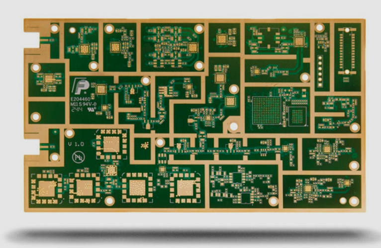
The practical arrangement is a small ceramic capacitor on the same side as the device, immediately next to the power pin, with its ground via adjacent to the device ground via. A bulk electrolytic at the input of the rail handles the slower load changes. Placing a capacitor at the input of a board’s power connector is a different measure again, and the values are chosen for the disturbance they have to absorb rather than by habit.
Protecting Analogue and Low-Level Inputs
An analogue input is almost always the victim, and the approach is to filter it as close to the point of entry as possible. A series resistor with a capacitor to analogue ground forms a low-pass filter whose corner frequency is set by the bandwidth the measurement actually needs. Placing the filter at the connector means the noise is removed before it can be coupled into anything else.
Where the input can see a voltage outside the supply range, clamping diodes protect the device, and a series resistor limits the current through them. The analogue and digital grounds under these components should be kept separate and joined only at the point defined by the grounding scheme, so the filter does not become a bridge that injects the digital return current into the analogue reference.
Cables, Connectors and the Outside World
A cable is an antenna, and it is usually the dominant coupling path in a system that passes its board-level tests and fails at the system level. Signal cables should be shielded where the environment is hostile, with the shield grounded to the chassis rather than to the signal ground at the connector end, and twisted pairs should be used for low-level signals so that the field couples equally into both conductors.
Physical separation inside the enclosure is a legitimate design measure. Power wiring should not run parallel to signal wiring for any distance, and where the two must cross, they should cross at right angles. The general rule is that a coupling path is proportional to the area it encloses, so every change that reduces that area reduces the interference, whether or not the mechanism is fully understood. For boards that combine a switching stage with a sensitive measurement, the measures described in the mixed-signal PCB design guidelines should be applied from the start rather than retrofitted.
FAQ
Is a ground plane split always necessary for mixed-signal boards? No. With a single continuous ground plane and a careful placement that keeps analogue and digital currents in separate regions, many mixed-signal boards work well without a split. The split helps when the digital return current is large and the analogue signal is small.
How do I choose the corner frequency of an input filter? From the bandwidth the measurement needs, not from the interference. Set the corner just above the highest frequency of interest, so that the filter has the maximum attenuation it can have without distorting the signal.
Are ferrite beads a substitute for good layout? No. A bead adds impedance in a specific frequency range and helps when a coupling path cannot be removed, but it also adds a resonance with the surrounding capacitance. Treat it as a supplement to layout and grounding measures rather than a replacement for them.