




PCB Design Constraints That Survive Manufacturing
Most PCB teams still hand down design rules as a table of fixed numbers: a minimum trace width here, a clearance there, a target impedance for every net on a given layer. That table works until the board stops being simple. Once a design carries several thousand nets and package pin counts climb past a couple of thousand, the document starts contradicting itself and the engineer has to decide which rule wins. Parametric PCB design constraints are the alternative. Instead of storing one number per rule, the tool stores the relationship behind the number and recomputes it whenever something else on the board changes.
Why Fixed Rule Tables Break Down
A fixed rule table is a snapshot of one design at one moment. When it was written, the stackup was known, the copper weight was known, and the etch capability of the fabrication shop was known. Six months later the same board moves to a different stackup for cost reasons, and every impedance-driven width in the table is now wrong. Geometry that produced 50 ohms on a 4.5 mil dielectric no longer does on a 3.8 mil one, but the table cannot tell you that. It keeps enforcing the old width, and the board ships with a controlled-impedance net that is twelve percent off target.
The same failure appears with clearance. A rule that says eight mil everywhere is a compromise, not a decision. Some nets need four mil to escape a dense ball grid array, while a 300 V switching node needs twelve mil or more. A single number forces the tight nets to be routed at a width they do not need, wasting routing channels that were already scarce, and leaves the high-voltage nets under-protected because nothing in the table distinguishes them. The rules sit in a spreadsheet, disconnected from the physics they were meant to capture.
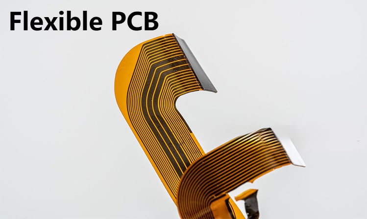
What Parametric Constraints Actually Encode
A parametric constraint stores the underlying process or electrical relationship instead of its current value. Trace width for a controlled-impedance net is stored as a function of dielectric thickness, dielectric constant, copper thickness, and the distance to the reference plane. Change the stackup and the tool recalculates the width, updates the rule, and flags every trace that no longer satisfies it. The designer reviews a short list of violations instead of re-deriving the entire geometry by hand, which is the difference between an afternoon and a week. Teams that already follow strict manufacturable design guidelines usually find this step is the one that finally makes those guidelines enforceable rather than advisory.
The same idea covers length matching. Rather than fixing all data lanes within 25 mil, the constraint can be expressed relative to the clock, with a tolerance that depends on the data rate and the dielectric. When the memory device changes from one speed grade to another, the tolerance tightens automatically and the affected traces are highlighted. Nothing has to be rediscovered, and no one has to remember why the old number was chosen.
Density, Pin Counts and Crosstalk
Modern packages are the reason this matters. A mid-range processor or FPGA easily presents 500 to 2,000 pins, and a single board can carry more than 5,000 nets, with more than half of them critical in some respect. Escaping that many connections from a 0.8 mm pitch array means the routing channels between the balls are the scarcest resource on the board. Every rule that is too conservative eats a channel that another net needed, and no fixed table can weigh those trade-offs.
Faster edges make the problem worse. As rise times shorten, crosstalk stops being a property of a single aggressor and becomes a cumulative effect across a bundle. A constraint that models coupled length, spacing, and layer assignment can hold crosstalk noise below a budget, while a fixed 3W spacing rule cannot tell the difference between a net that switches every two nanoseconds and one that switches once per frame. The relationship-based rule applies the tight spacing only where the timing actually demands it.
Benchmarking Against the Fabricator
Parametric rules only help if the numbers behind them reflect a real shop. Before a design is released, walk the constraint set through the fabrication house and confirm the minimum width, the impedance control tolerance, the minimum annular ring, the smallest drilled via, and the achievable dielectric thickness. Many suppliers quote a best-case figure that they can only hold on a two-layer board with heavy copper, and that number quietly becomes the basis of a constraint file on a far more demanding design. Getting the actual limits into the file prevents a board that passes local checks but cannot be built at the quoted price.
It is equally important to know how the shop measures. A trace width sized from a current calculation and quoted as a finished dimension after etching is not the same as the width drawn in the artwork, and the difference is a fixed offset that depends on copper weight. Once that offset is in the constraint model, the drawn width adjusts automatically. Without it, the same design comes back slightly high in resistance every time, and the discrepancy is blamed on the laminate.

When the Process Changes Mid-Program
A common scenario is a cost reduction between prototype and production. The board keeps its electrical function but moves to a cheaper laminate with a higher loss tangent, or the outer copper drops from two ounces to one. With fixed rules, the whole geometry has to be re-derived and re-verified, which typically takes days and often introduces new mistakes. With parametric rules, the stackup parameters are updated once and the tool recomputes widths, gaps, and impedance targets across every layer.
The team then runs a full design rule check to confirm the new process has not violated something else, such as a minimum annular ring, a spacing to the board edge, or a via-to-copper clearance that used to pass. The important change is that the check becomes a verification step rather than a rework step. Finding a violation inside the tool costs an hour, which is why teams that treat layout decisions as production decisions catch it there. Finding it after the first panel is etched costs a week, a new schedule, and a conversation with the customer.
What It Means for Prototype Builds
Prototypes are exactly where the old approach hurt most. A prototype exists to answer questions, and the fastest way to burn a cycle is to discover that the impedance is off spec or that a differential pair cannot be routed on the chosen stackup. When the constraint set is parametric, a prototype can be re-stacked and re-checked in an afternoon, which keeps the schedule tied to the experiment rather than to documentation cleanup.
It also changes how a team reviews a design. Instead of comparing the board against a static table, reviewers look at the constraint set itself: which relationships are encoded, which are still hard-coded, and whether the process assumptions are current. That is a far shorter conversation than tracing every net, and it catches the mistakes that a table-based flow hides until the fabricator pushes back.
The practical rule is simple. If a value can change when the stackup, the laminate, or the fabrication process changes, it should not be stored as a fixed number in a design rule document. Store the relationship, and let the tool do the arithmetic every time the design moves.
FAQ
Do parametric constraints replace a design rule check? No. They change what the check compares against. The design rule check still runs at the end of the layout; it simply evaluates recomputed values instead of a frozen table.
How many critical nets can a modern board really have? On a dense design it is common for more than half of the nets to be constrained in some way, and boards carrying 5,000 or more nets are routine once a large FPGA and its memory are included.
Is the setup effort worth it on a small board? On a two-layer board with a few hundred nets, a carefully written fixed rule table is usually enough. The payoff from parametric constraints starts when the layer count, the pin count, or the number of controlled-impedance nets grows.
Which constraint should be parameterized first? Controlled-impedance trace width, because it couples directly to the stackup and is the value most likely to change when the laminate or the copper weight changes.


