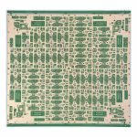
X-ray Inspection for BGA and Hidden Solder Joints
Optical inspection is excellent at finding what it can see. A missing component, a tombstoned chip, a solder bridge between two visible pins or a misaligned part are all obvious under a camera. What it cannot see is the underside of a ball grid array, where every joint is hidden between the package and the board.
That is the gap X-ray inspection fills. This article explains how the technique works, what the images actually show, which defects it finds reliably and which it does not, and how to use it as part of an inspection strategy rather than as a stand-alone answer.
What Optical Inspection Cannot See
A camera can only inspect a surface. Any joint that is formed underneath a package is invisible to it, and the same applies to the barrel of a plated through hole, the solder fillet beneath a large thermal pad and the internal structure of a package-on-package assembly. As packages have moved toward area array formats, the proportion of joints that are hidden has grown steadily.
For a ball grid array the situation is absolute: every electrical connection is on the underside. Automated optical inspection still has a role, because it verifies that the package is present, correctly oriented and within its placement tolerance, and it can detect a missing ball or a bridging defect at the edge of the array. It simply cannot confirm that the joints under the centre of the package are sound.
<img src="https://www.gopcba.com/wp-content/uploads/2025/09/金手指pcb.jpg" alt="X-ray image of a BGA solder joint array” />
How X-ray Inspection Works
The technique relies on the fact that materials absorb X-rays at different rates. Solder, which is a dense metal, absorbs far more than the laminate, the solder mask or the plastic of the package. When the board is placed between an X-ray source and a detector, the solder joints appear as dark features against a lighter background, and the image is effectively a map of the metal in the transmission path.
The resolution of the system is set by the size of the focal spot and by the geometry. A smaller spot and a closer source give a sharper image with more magnification, which is what allows a modern system to examine individual joints in a fine-pitch array. The same geometry causes the image to be a projection through the whole thickness of the board, which is the source of the technique’s main limitation.
Reading a BGA Image: Voids, Bridges and Opens
A good joint appears as a circular or slightly oval area of uniform density. A void appears as a lighter region inside it, because the empty space absorbs less radiation. A small amount of voiding is normal in a reflowed joint and is generally acceptable; a void that occupies a large fraction of the joint area reduces the thermal and mechanical path and is usually a reject.
An open connection appears as a joint that is thin, irregular or missing its connection to the pad, and a bridge appears as a continuous path of solder between two adjacent balls. Bridging is easier to see in the image than an open, because the density contrast is greater. Judging a marginal open requires an understanding of the process, which is why the inspection criteria should be agreed with the assembly house rather than invented at the machine.
Head-in-Pillow and Other Subtle Defects
The most difficult defect to detect is one where the solder ball and the paste have both reflowed but have not merged, leaving a joint that is in contact but not metallurgically continuous. The connection may pass a continuity test at room temperature and fail intermittently under thermal cycling or mechanical shock. In an X-ray image the sphere remains round rather than collapsing into the expected shape, which is the clue, but the image alone rarely proves the defect.
A related case is a joint that is fully formed but cracked, either within the bulk solder or at the interface. A crack may be visible as a fine lighter line at high magnification, particularly with a tilted view, but confirmatory analysis usually requires cross-sectioning the assembly. Recognising the limit of what imaging can prove is part of using it well.
Viewing Angles and Cross-Sectional Imaging
A straight-down view projects the whole board thickness onto one image, so structures on different layers overlap. Tilting the board, or using an oblique view, offsets the projections and separates features at different heights, which is what makes it possible to see a joint on one side of a package without the other side interfering.
Where the geometry allows it, the microstrip and stripline reference arrangements used for high-speed routing also define where a joint is most likely to be thermally stressed.
More advanced systems reconstruct a slice through the board, using multiple views taken from different angles. That provides a cross-sectional image at a chosen height and largely removes the overlapping problem, at the cost of longer scan times and more expensive equipment. For a dense area array assembly, the ability to examine one layer of joints at a time is often the difference between detecting a defect and guessing at it.
Inspection Strategy: Sampling or Full Coverage
Full X-ray inspection of every joint on every board is slow, and on a large panel it may not be practical at all. The usual approach is a risk-based one. The first articles of a new assembly are inspected in full, to confirm that the process is producing sound joints. Once the process is stable, inspection moves to a sampling plan that targets the highest-risk locations, such as the corners and centre of a large package and any component with a history of trouble.
Process changes bring the full inspection back. A new paste, a different reflow profile, a new package or a change of assembly line all invalidate the assumption that the process still behaves as it did when it was qualified. Applying the same logic used for component placement defects to hidden joints keeps the inspection effort where the risk actually is.
Limits of X-ray Inspection
Two limits are worth stating plainly. The first is that the image shows density, not electrical connection. A joint can look perfect and be open, and a joint can look marginal and be perfectly sound. X-ray inspection is a strong process-monitoring tool and a weak final-test tool, which is why it is normally combined with electrical test and with a functional check.
The second limit is throughput. A high-resolution scan of a dense area takes time, and the resolution required for a fine-pitch array is close to the practical limit of the technique. Where a design has many devices of that type, the inspection plan has to be built around sampling rather than around complete coverage, and the assembly house should be asked to state how it will verify the joints that are verified as part of the wider PCBA process rather than in isolation.
FAQ
Are voids in a BGA joint always a defect? No. Small voids are a normal result of the reflow process and are generally accepted. The concern is with voids that occupy a large fraction of the joint area, particularly at the interface with the pad, where they reduce the connection.
Can X-ray inspection replace electrical test? No. It confirms that the solder is present and reasonably formed, but continuity is an electrical property. A joint that is in contact but not fused can pass an image review and fail in service, so both checks are needed.
How often should a production line be X-rayed? Full inspection when the process is new or has changed, and sampling at the highest-risk locations once it is stable. The sample plan should be documented, and any change to paste, profile or package should reset it to full inspection.