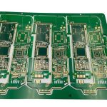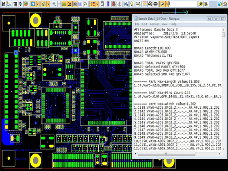
Stepped Board Fabrication: Cavity and Lamination Process
A stepped board is one whose surface is not flat. Part of the board is recessed, so that a component sits below the general surface level, or a cavity is opened so that a die, a sensor or an optical element can be mounted inside the board rather than on top of it.
The result is a local thinning of the stack rather than a uniform one, and that difference is what makes the process distinctive. This article follows the sequence from sub-assembly to finished outline, and points out the steps where a stepped board diverges from an ordinary multilayer.
What a Stepped Board Is For
The motivation is usually height. A product may need a component that is taller than the space available above the board, so the board is thinned locally to make room. In other cases the requirement is thermal or optical: a sensor that has to sit close to a lens, or a die that has to be mounted with a short thermal path to a metal base.
Whatever the reason, the design consequence is the same. The board has a region whose dielectric thickness and layer count differ from the rest, and the fabrication process has to create that region without damaging the layers that remain. That makes the step a stack-up decision before it is a routing decision.
Building the Sub-Assemblies
The stack is built from separate sub-assemblies rather than as a single block. An upper sub-assembly, one or more middle sub-assemblies and a lower sub-assembly are prepared separately, cut to size, and then imaged so that the circuit pattern is formed on the surfaces that will face inward once they are bonded.
Imaging is followed by the removal of the unwanted copper, which leaves the conductor pattern that will be buried inside the finished board. For the middle sub-assemblies the same step also creates the window: a region is routed out of the sub-assembly at the position and size where the cavity will eventually be, so that the opening already exists in the layers that will be inside the stack.

Alignment: Pins, Targets and Registration
Because the parts are made separately and then brought together, registration is the central problem of a stepped board. The usual solution is a set of alignment pins: holes are drilled in every sub-assembly at the same coordinates, and the stack is assembled over pins that pass through all of them. This guarantees that the sub-assemblies line up with each other mechanically rather than relying on optical alignment alone.
The pin positions have to be chosen so that they are inside the board outline and clear of the circuitry, and they have to be the same on every sub-assembly including any that will later be routed away. The registration achieved here determines the alignment between the cavity and the features on the layers above and below it, and that relationship can only be measured afterwards.
Resin Plugging Before Lamination
The alignment holes are drilled through every sub-assembly, and once the stack has been bonded they will pass through the finished board. Where those holes are not intended to remain as features, they are filled before the layers are joined, using resin plugging so that the drilled areas are closed and can be plated and imaged over like ordinary copper.
The filling has to be complete and free of voids, because a void left inside the stack becomes a trapped air pocket that expands during the press. The same sequence — fill, cure and planarise — is used for any via that would otherwise be exposed at an interface between sub-assemblies.
Lamination of the Stack
With the sub-assemblies prepared and the alignment holes filled, the layers are stacked with bonding sheets between them and pressed under heat and pressure in a vacuum press. The vacuum matters more than on a flat board, because air trapped in the cavity region has to be removed before the resin flows, otherwise the cavity walls will contain voids and delaminate later.
The press parameters also have to account for the reduced thickness in the step region. The pressure is applied over the whole panel, but part of the panel has less material resisting it, so the flow of resin into and out of the cavity area differs from the flow elsewhere. A stack that is not balanced around the cavity can distort as it cures. The balance of the stack-up and the arrangement of the bonding sheets are the two controls available.
Controlled Depth Routing to Open the Cavity
After lamination the cavity is still covered, because the upper sub-assembly was bonded over it as a continuous sheet. Opening it requires controlled depth routing: the router removes the material of the upper layer to a defined depth, stopping at the surface of the layer below so that the conductor pattern on that lower surface is exposed rather than cut.
Controlled depth routing is the critical operation of the whole process, because it has to remove the right amount of material across the entire cavity area while leaving the layer beneath intact. The tolerance on the depth is small in absolute terms, and the router has to compensate for the thickness variation of the bonded stack, which is not perfectly uniform. A cutter that removes too little leaves material in the cavity; one that removes too much destroys the layer that the cavity was meant to expose.
Second Drilling, Plating and Outer Layers
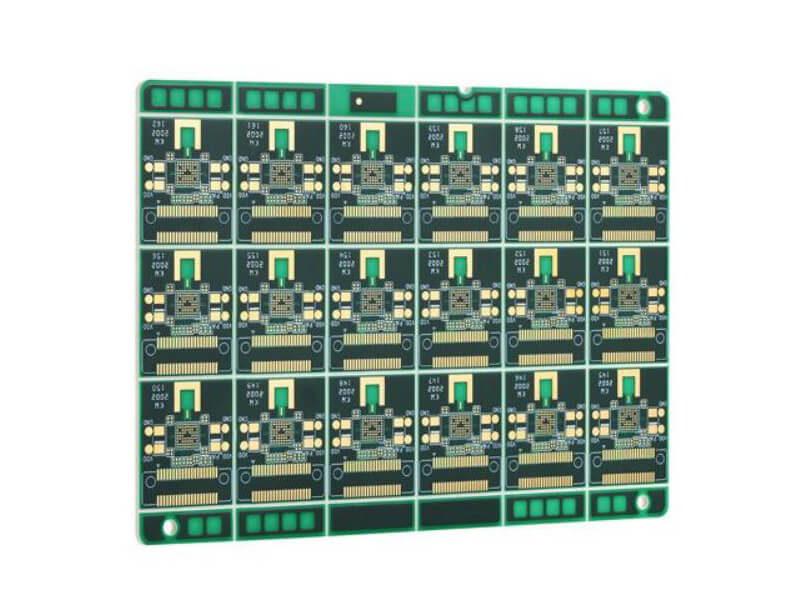
With the cavity open, the remaining holes are drilled. Slot cutters of different sizes may be used, because a stepped board often needs elongated openings as well as round holes, and the geometry of a short slot requires its own parameters, as described in the notes on short slot fabrication. All of the drilled features are then plated so that they conduct between layers, including the walls of the slots.
The outer layers are then formed by the normal route: a dry film resist is laminated over the plated panel, imaged and developed, the unwanted copper is etched away, solder mask is printed, and the legend is added. The difference from a flat board is that the process has to cope with the surface discontinuity at the cavity, which affects how the dry film conforms, how the mask is applied and how the panel is handled.
Tolerances and What to Specify
A stepped board has three tolerances that matter more than the rest. The first is the position of the cavity relative to the outer-layer features, which is set by the registration achieved during the alignment and lamination steps. The second is the depth of the controlled routing, which determines how much of the lower surface survives. The third is the flatness of the surface remaining after the cavity is opened.
All three belong on the fabrication drawing, along with the stack-up of the sub-assemblies and the lamination sequence. Because the process involves steps that an ordinary multilayer does not, it is worth discussing the design with the fabricator before the layout is finalised rather than after. The CAM preparation used for HDI work and the general design rules that keep a board manufacturable both apply, but the cavity tolerance and the routing depth are unique to this construction.
FAQ
Can a stepped board be made without a separate lamination sequence? The cavity has to be created by removing material after the stack is bonded, so the sequence is inherent to the process. A design that can tolerate a shallower step may be better served by a simpler construction.
What determines the depth of the step? The height that has to be accommodated, plus the thickness of the layers that must remain intact below the cavity. The two together decide how many layers have to be routed away.
Is a stepped board always more expensive than a flat one? Yes, generally, because of the extra sub-assembly handling, the alignment step, the second drilling operation and the controlled depth routing. It is justified where the mechanical or thermal requirement cannot be met any other way.