5G PCB Design Specification: Rules Before Layout
A design specification exists to remove decisions from the layout engineer without removing judgement. It fixes the inputs, the setup and the constraints that apply to every board the same way, so that the interesting part of the work — the placement and the routing of the critical nets — gets the attention it deserves.
This article sets out the rules that a 5G PCB design flow for a radio board typically contains, from the documents that have to be ready before layout starts to the checks that have to be completed before routing begins.
What a Design Specification Is For
A specification is not a checklist for its own sake. Its purpose is to make the design reproducible: two engineers applying the same document to the same schematic should produce boards that behave the same way, and a reviewer should be able to tell whether the rules were followed by looking at the layout rather than by asking.
That means the rules have to be concrete. A statement that decoupling should be placed close to the device is not a rule; a statement that the capacitor belongs within a defined distance of the supply pin and connects to a via immediately beside the pin is. The numbers can be adjusted for the design, but they have to exist.

Inputs: Netlist, BOM and Mechanical Drawing
Three documents have to be complete before layout begins. The first is the netlist, generated from a schematic that has passed its own review, so that the connectivity the layout inherits is correct. The second is a bill of materials in which every part has a defined footprint, because a part without a footprint will be discovered at the worst possible moment.
The third is the mechanical drawing. It has to show the board outline with tolerances, the position and size of every mounting hole, the position of every connector that mates with the enclosure or another board, and the areas where components may not be placed. New devices that have no established footprint should arrive with their package drawing attached rather than being researched during layout.
Setting Up the Board: Origin, Outline and Keep-Outs
The coordinate origin should be set to a defined mechanical reference rather than to whatever the tool defaults to. The intersection of the lower and left edges of the outline is the usual choice, and where the board is assembled into a frame, the first pad at the lower left corner is an alternative that makes the assembly data easier to interpret.
Corners of the outline are usually rounded, with a radius of a few millimetres, because a sharp corner is both a handling hazard and a stress concentration. Keep-out areas are defined in the same step: the region reserved for the panel edge and the clamping area used during assembly, the region occupied by standoffs or the inside of the enclosure, and any area near an antenna or a sensor where copper would change the behaviour of the part. All of these belong in the layout database rather than in a note.
Assembly Route as a Design Input
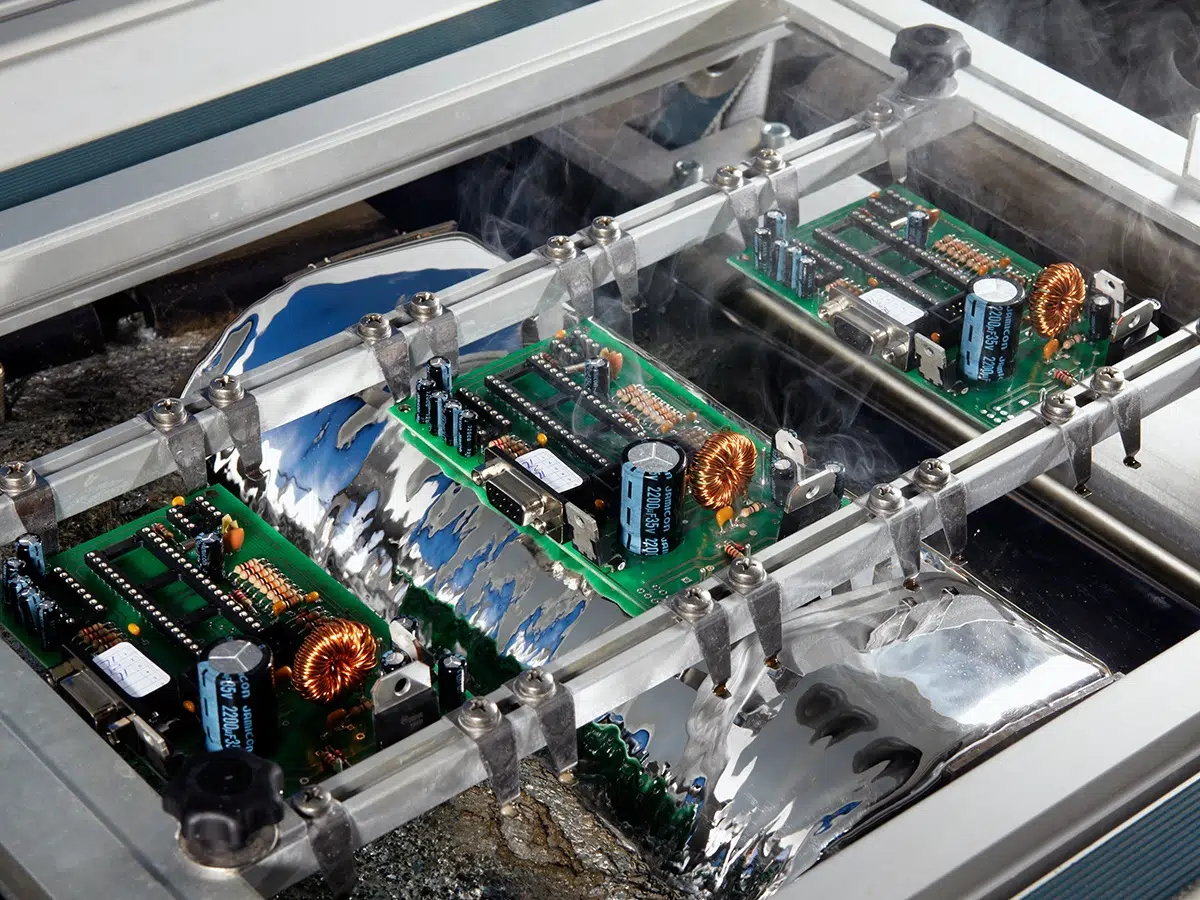
The assembly process should be chosen before the placement, because it constrains the layout. A board populated on one side only is the simplest to build, followed by a mixed assembly where through-hole parts are soldered in a single wave pass while the surface mount side is protected, then double-sided surface mount, and finally the combination where both a wave and a second reflow are needed.
The choice affects which side components may be placed on, how much space has to be left between parts, and the orientation of parts relative to the wave. Resistors and capacitors that will see the wave are normally oriented so that their axis is perpendicular to the direction of travel, while components with a fine pitch are kept off the wave side altogether, because a wave cannot reliably solder a pitch below about fifty mil.
Placement Rules: Order and Grouping
Placement follows a defined order: the parts that cannot move are placed first, then the core devices, then their supporting components, and finally the smallest parts. The parts that cannot move are those fixed by the mechanical drawing, and they should be locked as soon as they are placed so that a later move does not silently invalidate the mechanical fit.
Grouping follows the signal flow shown in the block diagram. Devices that form one function are placed together, high-voltage and high-current circuits are separated from low-level signals, analogue and digital sections occupy distinct areas, and high-frequency components are given adequate spacing. Where the same circuit is repeated, a symmetrical arrangement of the repeats makes both the placement and the review easier.
Net Classes and Constraint Setup
Once the placement is settled, the nets are sorted into classes that share a set of electrical and physical requirements. A class is defined by what the nets have in common: a supply rail, a differential pair, a clock that has to reach several devices with matched delay, or a set of analogue signals that must not pick up switching noise, in the way the mixed-signal layout guidelines set out. Every net belongs to exactly one class, and every class carries rules that the router can enforce.
The rules attached to a class are the numbers that the review will check. A supply class carries a minimum trace width derived from the current it has to carry, a via count limit and a requirement that the return path is continuous. A differential class carries a target impedance, a maximum intra-pair skew measured in length rather than time, and a spacing rule that has to be held over the whole route rather than only at the ends.
Layer Assignment and Impedance Targets
The stack-up decides which layers the classes may use. Planes are reserved and are not routed on except where a controlled impedance reference is required, and the layers next to a plane are kept for the nets that need a defined reference or the best immunity. The assignment is made before routing begins because a net moved from one layer to another after the route is drawn acquires a different impedance and a different return path.
Impedance targets are calculated from the stack and recorded per layer, because a single target cannot apply to a trace on an outer layer and to one buried between two planes. Preserving the reference across a layer change is part of the same discipline, and the return via that has to accompany a signal via is a rule that belongs in the specification rather than in the router’s judgement.
Checks Before Routing Begins
The last stage of the specification is the set of checks that have to pass before the routing is allowed to start. The netlist is compared against the schematic, the placement is compared against the mechanical drawing and against the keep-outs, and the classes are checked for nets that were left unassigned. A net that belongs to no class will quietly be routed with default rules.
These checks are cheap when they are run at this stage and expensive when they are run later. A misplaced connector discovered after the routing is complete costs the routing; the same connector discovered during the placement costs a few minutes. The design rules that keep a board manufacturable and the order used to place the parts are the two documents this stage depends on most.
FAQ
Who owns the design specification? The layout engineer is usually the author and the owner, because the document exists to guide the layout. The electrical engineer contributes the electrical rules and the mechanical engineer the outline, but one person has to hold the document together.
Should the specification be complete before layout starts? The parts that affect the placement and the stack-up have to be settled first, because those decisions are expensive to reverse. Rules that only affect the routing can be added as the classes are prepared.
How are the rules enforced? Where the tool supports net classes with attached rules, the router checks them automatically and reports violations. Where it does not, the rules are enforced by review, which is why the numbers have to be recorded rather than remembered.