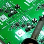
Flying Probe Testing: What It Catches and When to Use It
Electrical test is the last chance to find a defect before a board leaves the factory, and it answers a question that no amount of visual inspection can. A board can look perfect and still have an open circuit, a short between two nets, or a connection to the wrong net, and none of those is visible. Flying probe test is the method that finds them without a dedicated fixture, which is why it is the default for prototypes and small batches.
What Electrical Test Is For
The purpose of a bare board electrical test is to compare the board against the netlist it was designed from. Every net should be continuous from end to end, and no two nets should be connected. That is the entire specification, and testing it catches the failure modes the fabrication process produces: an open trace from an etch defect, a short from residual copper or a plating bridge, and a misregistered layer that connects the wrong pads.
The test says nothing about impedance, about solderability or about appearance. It is a continuity check against the design data, and its value lies in being exhaustive where a visual check is not. Every net on the board is tested, including the ones buried between layers where nothing can be seen at all.
How a Flying Probe System Works
A flying probe machine carries a small number of independently controlled probes, typically four to eight, mounted on linear motors. The board is loaded, positioned and clamped, and the probes then move to each test point in turn rather than being fixed in place by a fixture. Each probe is connected through a multiplexing system to the drivers, which may be signal generators or power supplies, and to the sensors, which may be digital multimeters or frequency counters. While one component or net is being measured, the rest of the board is electrically isolated by the remaining probes so that the reading is not disturbed.

What It Catches
A flying probe test compares the board with the netlist, so the defects it finds are the ones that break that comparison. An open circuit, where a net is not continuous from one end to the other, is found immediately. A short circuit between two nets that should be separate is found in the same pass. A board whose layers are misregistered so that a pad connects to a neighbouring net shows up as an unintended continuity, which is the defect that is hardest to see and easiest to ship.
Because the probes touch every test point, the test also confirms that the drilled holes and the plated barrels connect the layers they are meant to connect. A barrel that has not plated through is an open circuit between two layers, and it is invisible from both surfaces.
Flying Probe versus Fixture Test
A fixture based in-circuit tester uses a bed of nails, one pin per test point, held in a plate built for that board. Once the fixture exists, testing is fast: the board is pressed down and all the nets are measured at once. The cost is the fixture itself, which has to be designed, drilled and assembled, and which is only worth building for a product that will be produced in volume.
A flying probe needs no fixture. That removes the tooling cost and the lead time, and it means a design can be tested on the first article and retested after every change without new tooling. The trade is time per board, because the probes move serially from point to point. For a prototype or a small batch the total cost is lower; for a run of thousands, the fixture pays for itself quickly.

The choice between the two methods is usually not exclusive. A product that starts on flying probe as a prototype can move to a fixture when volumes justify the investment, using the same test program and the same access points. What matters at the design stage is simply that the nets are reachable, because that is the decision which cannot be revisited later without changing the layout.
It is also worth remembering what the test does not cover. Continuity says nothing about whether the impedance of a controlled trace is correct, whether a solder mask is properly cured, or whether the board will survive thermal cycling. Those are process questions, verified by coupons and microsections rather than by electrical test, and a good test result is not evidence that they were answered.
Design Rules That Make Test Possible
The test can only reach what the design exposes. A net with no accessible pad cannot be probed, and a pad that is covered by a component cannot be reached by a probe that approaches vertically. Test points are therefore a design decision, and they are cheapest to add while the layout is being made rather than after the first article fails to test.
Two rules cover most of it. Give every net that would otherwise be inaccessible a test pad, and place those pads where a probe can land without obstruction, which means away from tall components and clear of the board edge. The pads should be a size the machine can hit reliably, and their positions should be included in the test program rather than discovered from the artwork. Where a board will be produced in volume, a bed of nails built later needs the same points, so nothing is wasted by designing them in from the start.
Where Test Sits in the Flow
Bare board test sits between fabrication and assembly, and it is the last checkpoint at which a fabrication defect can be caught cheaply. A short or an open found at this stage costs a board. The same defect found after components have been placed and reflowed costs the board, the components and the assembly time, and if it reaches the field it costs considerably more than that.
That is the argument for testing electrical continuity on every board rather than sampling it, and it is also the argument for keeping the test program current. A test program that lags behind the design tests the wrong netlist, which is worse than no test at all because it produces a pass that means nothing. The overall expectations for a delivered board are set out in PCB design quality characteristics, and the points worth fixing with the fabricator at the prototype stage are covered in multilayer PCB prototype requirements. Where the same board goes on to assembly, the flow that includes electrical test is described in PCBA development process.
FAQ
What does flying probe testing actually verify? Continuity against the netlist: that every net is complete from end to end, that no two nets are connected, and that the plated holes connect the layers they were designed to connect.
Why use flying probe rather than a bed of nails? Because it needs no fixture. That removes the tooling cost and the lead time, which makes it right for prototypes and small batches. Fixture test is faster per board and wins in volume.
Can flying probe test measure component values? It can measure components on an assembled board, but on a bare board its purpose is continuity. Extended capability such as boundary scan or device programming depends on the system and the options fitted.
What happens if a net has no test point? It cannot be probed, so a defect on that net passes the test. Test points are a layout decision, and adding them after the layout is finished costs more than placing them during it.