Heavy Copper PCB: Design Rules for 2 oz and Above
A heavy copper PCB is used where the board has to carry current that an ordinary trace cannot, or where it has to move heat away from a component into a wider area. Two ounces per square foot is the usual starting point, and designs that reach four or six ounces appear in power supplies, motor drives, battery management and welded assemblies. The electrical benefit is easy to describe and the manufacturing consequences are not.
What Heavy Copper Is For
The first reason to specify it is current. A trace of a given width carries roughly twice the current at two ounces that it carries at one, for the same temperature rise, which means the same circuit can be built in less area or run cooler in the same area. The second reason is thermal: a heavy copper layer spreads heat laterally before it has to cross the laminate, which lowers the temperature of a hot component and of its neighbours.
The third reason is mechanical. A heavy copper layer stiffens the board, which helps where a connector or a large component has to be supported, and it allows a busbar or a solder-in shunt to be replaced by copper on the board. Where a design combines all three, the case for heavy copper is usually clear before the tooling is ordered.
Current and Temperature Rise
The current capacity of a trace is not a property of the trace alone. It depends on the copper weight, the width, the permitted temperature rise, the position of the layer and the amount of copper around it. A trace on an outer layer with a large copper pour beside it behaves differently from an isolated inner layer trace of the same geometry, and the difference is large enough that a table cannot be applied without judgement.
The calculation is usually made against a permitted temperature rise rather than against a fixed current, and then checked for voltage drop, because a trace can be thermally acceptable and still lose too much voltage on a low voltage rail. The relationship between width, thickness, current and temperature is set out in trace width and current calculation, and the heavy copper case should be evaluated with the fabricator rather than assumed.
Heat Spreading
Where heavy copper earns its cost most clearly is in the thermal path. A component dissipating several watts transfers heat into the copper beneath it, and that copper then has to spread the heat to an area large enough that the laminate and the air can carry it away. Thicker copper spreads heat further and lowers the local temperature, which extends component life.
Thermal vias connect the spreading copper on the surface to copper on other layers and to a heat sink behind the board. Their effectiveness depends on the copper they connect to: a via array landing on a thin signal layer achieves very little, while the same array landing on a heavy plane acts as a proper thermal connection. Filling or capping the vias is often required so that solder does not wick away during assembly.
Fabrication Limits
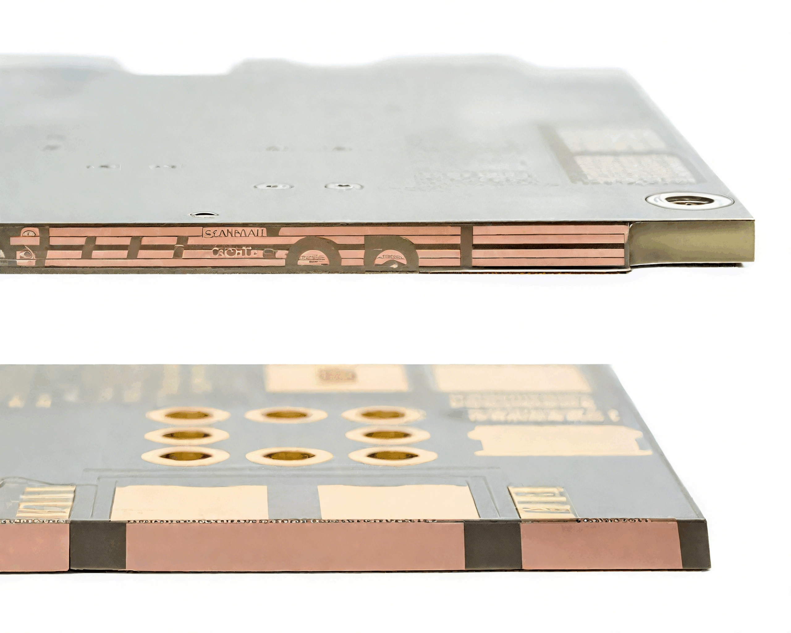
Etching is the first constraint. The etchant removes copper sideways as well as downwards, so a thick layer produces more undercut and a cross section that is far from rectangular. The minimum line width and spacing that can be held therefore increase with the copper weight, and a design that needs fine lines should place them on a lighter layer rather than insisting on fine geometry in heavy copper.
Plating and lamination follow. Vias have to be plated in the same bath as the heavy surface copper, and a thick deposit on the surface can close the hole before the barrel is properly coated. Lamination must fill the spaces between heavy copper features with resin without leaving voids, which is why the fabricator adjusts the press cycle and sometimes the resin content of the prepreg for a heavy copper design. The chemistry that controls how the copper fills a via is described in electroplating additives, and the way the stack behaves through the press is covered in PCB dimensional stability and expansion.
Design Rules
Decide which layers carry the heavy copper and keep the fine geometry on the others. Give the heavy features generous spacing so that etching can remove the copper between them, and avoid isolated small features in a heavy layer because they are the first to be lost to over etching. Where a heavy layer is used as a plane, it also acts as a heat spreader and as a mechanical stiffener, so the copper balance of the stack should be planned rather than left to chance.
Mixed weights in one stackup are normal. A four layer board might use one ounce on the outer signal layers and two or three ounces on an inner power layer, or a two layer board might use two ounce on both faces. The amplifier must be described layer by layer on the fabrication drawing, because the panel plan and the process parameters depend on it.
Assembly and Handling
Heavy copper boards are heavier and stiffer, and they retain heat differently during soldering. The thermal mass means that a reflow profile developed on a standard board will not transfer directly, and the preheat has to be long enough to bring the whole assembly to temperature without overheating the surface. This is particularly relevant where the board also carries a heavy internal plane.
Solder joints to a heavy copper pad also cool faster in one sense and slower in another: the copper conducts heat away from the joint as it forms, which can produce a joint that looks correct but has not fully wetted. Where a large copper area is soldered to a component, thermal relief spokes or a divided pad help the soldering process, at the cost of some electrical and thermal performance.
Verification
Inspection of a heavy copper board concentrates on the geometry that the process struggles to hold. Copper thickness is verified on a coupon, the etch factor is checked by measuring a test pattern, and the plated barrels are examined by microsection. Where the board carries a thick plane, the laminate between the heavy features is inspected for voids and resin starvation, which a simple visual check will not reveal.
Electrical verification then confirms the two properties the design was built for: the resistance of the power path and the thermal behaviour under load. A thermal image taken with the board operating at full current will show whether the copper is spreading heat as intended, and it is a more informative test than a continuity check on a design of this kind.
FAQ
How thick can heavy copper go? Two to four ounces is routine for power work, and thicker layers are produced for specialised applications. The achievable feature size falls as the weight increases.
Can fine lines be combined with heavy copper? Only within the wider minimum geometry that heavy copper allows. Where fine lines are needed, they belong on a separate, lighter layer.
Does heavy copper improve high frequency performance? Not directly. It affects impedance through its thickness, and the etch profile of a heavy layer makes tight impedance tolerance harder to hold.