PCB Dimensional Stability and Expansion Control
A printed circuit board is a laminate of materials with different thermal and mechanical properties, pressed together under heat and then subjected to a series of wet processes and thermal cycles. Each of those steps changes the dimensions of the panel, and the accumulative change is what the industry calls expansion and contraction, or growth and shrinkage. The tolerance that results is not a manufacturing failure; it is a physical property of the material, and it has to be designed for.
Where the Change Comes From
The base material expands when heated and contracts as it cools, and the expansion coefficient along the glass fibres differs from the coefficient across them. Copper expands as well, and it is bonded to the laminate, so the two constrain each other. During lamination the resin flows and cures, and the resulting internal stresses are released gradually as the panel passes through subsequent process steps.
Moisture is the second mechanism. Laminate absorbs water from the atmosphere and from the wet processes, and the absorbed moisture changes the dimensions of the panel. When the panel is subsequently heated, for example during drilling or assembly, the moisture leaves and the panel shrinks. This is why boards are baked before certain operations, and why the storage conditions of a panel affect its dimensional behaviour.

Material Selection and Its Effect
Materials differ substantially in how much they move. A metal-backed board, in which a metal core carries the laminate, is thermally stable and shows a small expansion for a given temperature change, which is why the technique is used for circuits that carry high power. A standard glass reinforced epoxy expands more, and the coefficient is anisotropic because of the fabric orientation.
High-frequency laminates behave differently again. They are often filled with ceramic particles to reduce the dielectric constant and its variation with temperature, and the filler also changes the mechanical behaviour. Material selection is therefore a dimensional decision as well as an electrical one, and its interaction with the stackup is described in this article on layer stackup design.
Process Steps That Move the Panel
The fabrication sequence contains several steps that change dimensions. The lamination press is the largest, since it applies both heat and pressure and locks in the residual stress of the stack. Drilling follows, and the accuracy of the hole position relative to the copper pattern depends on how much the panel has moved since the inner layers were imaged.
Etching removes copper and changes the local stress balance, which is one reason why dense and sparse areas behave differently. Plating adds copper and resists expansion. The final thermal excursions during assembly then release stress that has accumulated, and the panel may move again.
The consequence for the designer is that the clearance between a hole and the copper around it must account for movement during every one of those steps, and not only for the accuracy of the drill. The arithmetic of that tolerance stack is set out in this discussion of via to trace clearance.
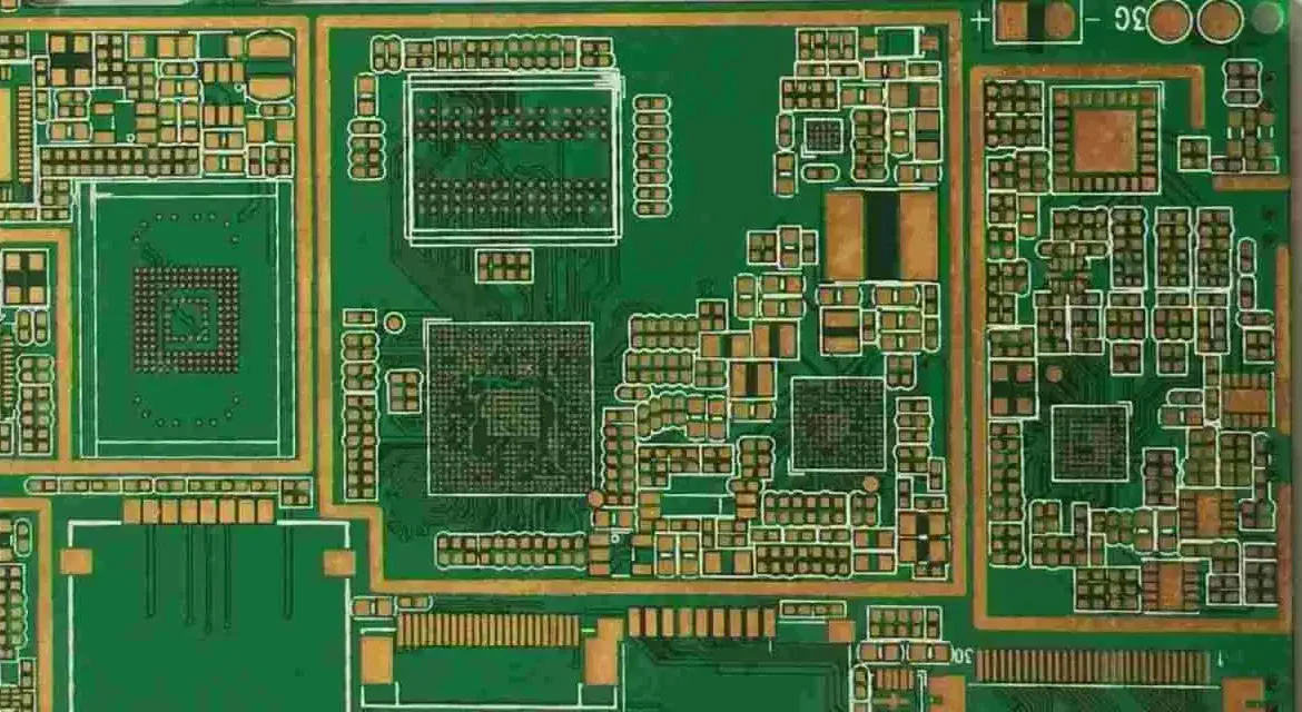
<img src="https://www.gopcba.com/wp-content/uploads/2024/09/Standard-PCB.jpg" alt="layer registration marks used to verify dimensional stability” />
Layer Registration
Layer registration is the measure of how accurately the copper features on one layer line up with those on the layers beneath. It is checked with registration marks at the panel corners and sometimes in the interior, and the measured value determines whether the clearances the designer specified have actually been achieved.
Registration errors are not uniform. A panel may be within tolerance at the centre and outside it at the edges, because the movement during lamination is a combination of uniform shrink and local distortion. A design that places its tightest clearances at the panel edge is therefore exposing them to the least favourable conditions.
Where a design is built on a material with a large expansion coefficient, or where the panel is large, the fabricator may allow a greater registration tolerance. Layered into that tolerance is the requirement that the annular ring around a hole remain adequate after the movement, which is why pad sizes for such constructions have to be larger than the minimum.
Process Control
The fabricator controls expansion by controlling the process. Temperature ramps in the lamination press are profiled so that the resin cures uniformly, and the press cycle is designed to minimise residual stress. The panel is baked before drilling to remove moisture, so that the drilling occurs at a known moisture content rather than at whatever the ambient humidity produced.
Compensation is the other tool. By measuring how much a particular construction moves, a fabricator can scale the artwork so that the finished dimensions land on the target, and this pre-compensation is standard practice on high-layer-count boards. The compensation is specific to a material, a stack and a process, which is why a design transferred between suppliers often has to be re-qualified.
Designing for Dimensional Change
The practical measures are straightforward. Provide adequate clearance so that movement does not consume the annular ring. Place the tightest geometries toward the centre of the panel rather than at its edge. Specify a material whose dimensional behaviour is appropriate to the requirements rather than one chosen only for its electrical properties. And confirm with the fabricator what registration tolerance the construction can hold, since that figure, rather than the nominal drill accuracy, is what the design actually has to live with. The wider topic of how design data and process capability interact is discussed in this article on PCB design and fabrication.
Thermal Expansion During Assembly
Thermal expansion does not end when the board leaves the fabricator. During assembly the whole panel is heated to the reflow temperature and then cooled, and the laminate expands and contracts by an amount that depends on the material and on the direction of the glass fabric. The copper on the surface expands less in the plane of the board but exerts its own constraint on the resin, and the result is a small but measurable change in dimension each time the board passes through an oven.
The same effect operates at the level of an individual joint. A plated hole connects copper on several layers, and when the board is heated those layers move relative to one another. The barrel of the hole has to accommodate that movement, which is why plating ductility matters, and why a hole plated with brittle copper can crack during assembly even though it passed every test beforehand. The relationship between plating quality and the geometry around the hole is described in this article on copper plating defects.
FAQ
Is board growth a defect? No, it is a physical property of the materials. Laminate expands with temperature and changes dimension with moisture content, and copper and resin move by different amounts. The fabricator compensates for the expected movement, and the design has to tolerate the residual variation.
Why is a panel baked before drilling? To remove absorbed moisture so that the panel is drilled at a known and consistent moisture content. Without the bake, the drilling accuracy varies with the ambient humidity, and the panel may shrink further during later thermal processing.
How much clearance should be allowed for registration error? Enough that the annular ring around each hole remains adequate after the worst-case movement. The figure should come from the fabricator for the specific material and stack, since it depends on the construction rather than on the drill alone.